Popular Keywords
Intel
News
[News] Intel Won’t Discontinue Raptor Lake DDR4 Models, Supports Lower-Memory Configurations Amid Shortages
Intel says it is taking steps to address ongoing memory supply constraints. According to Tom’s Hardware, when asked how the company is responding to constrained memory supply, Nish Neelalojanan, senior director of product management for Intel’s Client Computing Group, cited Raptor Lake and Wildc...
News

[News] Intel Lip-Bu Tan Reflects on Taiwan’s Semiconductor Journey, Highlights AI and 18A Roadmap at COMPUTEX
As AI shifts from training to inference, CPUs are once again taking center stage in the industry, putting Intel firmly back in the spotlight. Intel CEO Lip-Bu Tan's appearance at COMPUTEX has therefore drawn significant attention. According to Economic Daily News, Tan used his keynote to outline In...
News

[News] Intel Advances Glass Substrate Push with 3DGS, US$3.3 Billion India Plant Set for Five-to-Six-Year Buildout
Intel is moving ahead with its glass substrate push. According to Reuters, the Indian government said Intel and 3DGS plan to invest about US$3.3 billion to build a substrate manufacturing plant in Odisha, eastern India. The planned plant will be built in the Bhubaneswar-Khurda region over five to si...
News

[News] COMPUTEX 2026 Preview: From Intel Budget AI CPUs to CPO Momentum Fueled by NVIDIA Vera Rubin
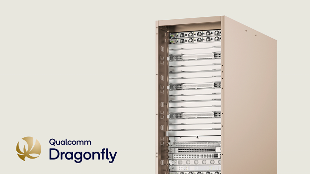
COMPUTEX is set to take place from June 2 to June 5. The event will bring together CEOs from companies, including Qualcomm and Intel, along with senior executives from nearly 30 firms, as noted by Central News Agency. The lineup spans the full AI ecosystem and represents more than US$10 trillion in...
News
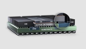
[News] Intel Reportedly to Adopt Silicon Capacitors in 2027 to Improve EMIB Power Stability for Google’s v8e
With TSMC’s CoWoS capacity remaining constrained, Intel’s EMIB (Embedded Multi-die Interconnect Bridge) advanced packaging technology is increasingly gaining traction as an alternative, fueling expectations for stronger demand across related components. Notably, ZDNet reports that Intel plans to...
- Page 3
- 104 page(s)
- 517 result(s)