Popular Keywords


DRAM
Insights

[Insights] Memory Spot Price Update: DRAM Spot Prices See Gains in Low-Density DDR4 and DDR3 Amid Sideways Market
According to TrendForce’s latest memory spot price trend report, DRAM spot prices this week have seen upward momentum in low-density DDR4 and DDR3 segments, while the broader market continues to trend sideways. In NAND Flash, suppliers are adjusting quotations to optimize inventory levels, but buy...
News

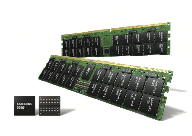
[News] Samsung, SK hynix 800 Trillion Won Expansion Strains Chipmaking Tool Supply, Potentially Pressures TSMC, Intel
The global semiconductor industry is set to enter a new Warring States era, as Samsung Electronics and SK hynix unveiled a sweeping investment push in South Korea. According to The Elec, the two memory giants will jointly deploy 800 trillion won to build four new fabs in the country’s southwest, a...
News

[News] Asian Memory Makers Turn to U.S. Capital Markets: SK hynix and Kioxia Advance ADR Plans
As AI-driven memory demand continues to outpace supply, leading Asian memory makers are accelerating capital market strategies to support large-scale expansion. Notably, SK hynix and Kioxia have both advanced plans to issue U.S. depositary receipts (ADRs), underscoring a broader push to tap U.S. inv...
News

[News] Lenovo Reportedly Sees Higher Memory Prices Becoming the New Normal Into 2030
As Micron noted in its earnings call that tight market conditions are likely to persist beyond 2027, Lenovo is taking a more cautious stance. Wccftech, citing company management, reports that Lenovo sees higher memory pricing as potentially settling into a “new normal” well into 2030 and beyond....
News
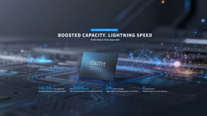
[News] Micron Reportedly Acknowledges China’s Memory Progress While Noting Output Remains Largely Domestic
Amid market chatter that big tech firms are reportedly evaluating Chinese memory products, Micron, during its earnings call, acknowledged the country’s progress in memory development. South China Morning Post, citing Micron Chief Business Officer Sumit Sadana, reports that both CXMT and YMTC have ...
- Page 1
- 144 page(s)
- 716 result(s)