Popular Keywords


Wafer Foundries
News
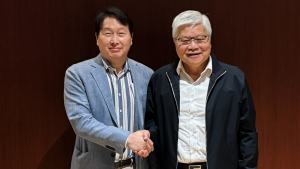
[News] SK Group Chair Chey Tae-won Meets TSMC Chairman C.C. Wei After Two Years, HBM, Advanced Packaging in Focus
Shortly after touring SK hynix’s COMPUTEX booth in Taipei alongside NVIDIA CEO Jensen Huang on June 2, SK Group Chairman Chey Tae-won met with TSMC Chairman C.C. Wei for the first time in two years, according to a post by SK hynix on its official X account on June 4. Hankyung adds that the meeting...
News

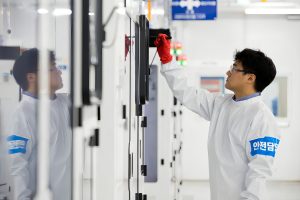
[News] Intel Reportedly Scales EMIB Expansion in U.S., Vietnam, with Taiwanese Tool Orders Set for 2H26 Delivery
As Intel’s EMIB (Embedded Multi-die Interconnect Bridge) advanced packaging gains traction and draws strong market attention, the company is reportedly accelerating capacity expansion globally. An Investor.com report suggests Team Blue is advancing EMIB capacity expansion in parallel, with its Ore...
News
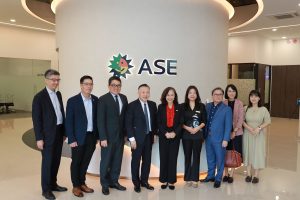
[News] ASE, Powertech, KYEC CapEx May Hit NT$370B This Year as AI Drives Record OSAT Investment
The AI chip race is intensifying across the board, with advanced packaging growing in significance and driving a surge in OSAT capital spending. According to Commercial Times, Taiwan-based OSAT players ASE, Powertech, and King Yuan Electronics (KYEC) are expected to see their combined capital expend...
News
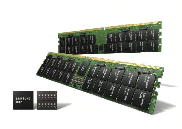
[News] Samsung’s May Strike Seen Disrupting Up to 4% of DRAM Output, With Weeks-Long Recovery Risk
As global memory supply remains extremely tight amid the AI boom, Samsung’s looming large-scale strike is seen as further intensifying the strain. According to South Korean media outlets News1 and The Dong-A Ilbo, citing analysts, disruptions could reach 3–4% for DRAM and 2–3% for NAND, based ...
News

[News] TSMC Advances Panel-Level Packaging, CoPoS Pilot Line Reportedly Set for June Completion, 2028–29 Ramp Eyed
Ahead of TSMC’s earnings call later this week, the spotlight is once again on its advanced packaging roadmap—and CoWoS is no longer the only story. According to Commercial Times, TSMC’s CoPoS (Chip-on-Panel-on-Substrate) pilot line has already begun tool deliveries to R&D teams in February...
- Page 1
- 29 page(s)
- 141 result(s)