Popular Keywords


未分類
News
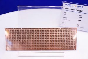
[News] China Advances TGV Glass Substrate Tech as BOE, ECHINT, and Peers Step Up
According to ijiwei, citing CNpowder, as chip packaging technology advances rapidly, glass substrate TGV (Through Glass Via) has emerged as a focal point of industry attention. Glass substrates are gaining attention for their superior heat dissipation, conductivity, and flatness. As noted by Commer...
News

[News] Samsung’s First Android XR Headset ‘Moohan’ Reportedly Set for Late October Launch
More details about Samsung’s first XR device have surfaced. Until now known as ‘Project Moohan,’ the device reportedly marks the tech giant’s first Android-based XR headset, developed in partnership with Google and Qualcomm. According to the Chosun Daily, the new device is slated for release...
News
[News] Google’s Hardware Play: AI in Focus, Flip-Style Foldable and Tablet Can Wait
Google just unveiled its latest Pixel 10 series. According to TechNews, citing Bloomberg, the company said it currently has no plans to launch a flip-style foldable and that its tablet project remains on hold. Pixel Design, AI Push, and Flip-Style Foldables on Hold Google’s design chief, Iv...
News

[News] Apple’s First Foldable iPhone Set for 2026 as Hinge Suppliers Compete
Apple is expected to launch its first foldable smartphone in 2026, and competition among potential component suppliers is already intensifying. According to Patently Apple, which cited a well-known analyst, Samsung Display is likely to supply a crease-free display solution for the device. Meanwhile,...
News

[News] Subsidies Spark Surge: iPhone 16 Pro Reportedly Tops China’s Sales Charts Last Week
Apple’s iPhone 16 Pro has grabbed major attention after joining China’s national consumer subsidy program for the first time, as highlighted by technode. Now, a CNA report suggests that riding this wave and the 618 shopping festival, the model has soared to the top of smartphone sales in China. ...
- Page 1
- 7 page(s)
- 33 result(s)