IC Manufacturing, Package&Test


2024-02-01

[News] Intensified Competition in the Semiconductor Industry for 2nm Technology Dominance, Potentially Reshaping the Global Foundry Market

The competition for dominance in 2nm semiconductor technology has intensified at the beginning of 2024, marking a crucial battleground among global foundry companies.

As per a report from IJIWEI, major foundry enterprises such as Samsung Electronics, TSMC, and Intel are set to commence mass production adopting 2nm process starting this year. Consequently, the fierce competition for supremacy in 2nm technology is expected to escalate from 2025 onwards. Currently, the most advanced production technology globally is at the 3nm level.

  • TSMC

TSMC’s 2nm products will be manufactured at the Fab 20 in the Hsinchu Science Park in northern Taiwan and at a plant in Kaohsiung.

The Fab 20 facility is expected to begin receiving related equipment for 2nm production as early as April, with plans to transition to GAA (Gate-All-Around) technology from FinFET for 2nm mass production by 2025.

During TSMC’s earnings call on January 18th, TSMC revealed that its capital expenditure for this year is expected to fall between USD 28 billion and 32 billion, with the majority (70% to 80%) allocated to advanced processes. This figure is similar to that of 2023 (USD 30.4 billion), indicating stable investment to ensure its leading position in 2nm technology.

  • Intel

After announcing its re-entry into the foundry business, Intel is actively advancing its foundry construction efforts. The plan includes the introduction of the Intel 20A (equivalent to 2nm) process in the first half of 2024 and the Intel 18A (1.8nm) process in the second half of the year. It is understood that the Intel 18A process will commence test production as early as the first quarter of this year.

Intel’s 2nm roadmap is more ambitious than originally anticipated, being accelerated by over six months. In response to criticisms of its “overly ambitious” plans, Intel swiftly began procuring advanced Extreme Ultraviolet (EUV) equipment.

  • Samsung Electronics

Samsung Electronics has devised a strategy to gain an advantage in the more advanced process war through its Gate-All-Around (GAA) technology. Currently, it is mass-producing the first-generation 3nm process based on GAA (SF3E) and plans to commence mass production of the second-generation 3nm process this year, significantly enhancing performance and power efficiency.

Regarding the 2nm process, per a report from Nikkei, Samsung plans to start mass production for mobile devices in 2025 (SF2) and gradually expand to high-performance computing (HPC) in 2026 and automotive processes in 2027.

Currently, Samsung Electronics is producing GAA products for the 3nm process at its Hwaseong plant and plans to manufacture products for both the 3nm and 2nm processes at its Pyeongtaek facility in the future.

  • Rapidus

Rapidus, a chip manufacturing company supported by the Japanese government, is expected to trial-adopt 2nm process at its new plant by 2025 and begin mass production from 2027.

If Rapidus’ technology is validated, the global foundry market may expand beyond the Taiwan-Korea duopoly to include Taiwan, Korea, the United States, and Japan.

The technology competition to become a “game-changer” ultimately depends on the competition for customers. It’s rumored that TSMC holds a leading position in the 2nm field, with Apple speculated to be its first customer for the 2nm process. Graphics processing giant NVIDIA is also considered a major customer within TSMC’s client base.

According to TrendForce data as of the third quarter of 2023, TSMC’s revenue share accounted for a dominant 57.9%, with Samsung Electronics trailing at 12.4%, a gap of 45.5 percentage points.

However, Samsung Electronics is not sitting idly by. With continuous technological investment, Samsung’s foundry customer base grew to over 100 in 2022, a 2.4-fold increase from 2017. The company aims to expand this number to around 200 by 2028.

Particularly, Samsung’s early adoption of GAA technology is expected to give it an advantage in achieving early production volumes for advanced processes.

Read more

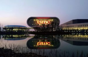
(Photo credit: TSMC)

Please note that this article cites information from IJIWEI and Nikkei.

2024-01-23

[News] Subsidies from the U.S. Legislation “NAPMP” Potentially Expected to Cover IC Substrates

The U.S. Department of Commerce has initiated the “National Advanced Packaging Manufacturing Program (NAPMP) ,” with materials and substrates being the first subsidized areas. Due to the close collaboration between IC testing and IC substrates, it is not ruled out that the IC substrate industry could be the next recipient of subsidies under the U.S. chip legislation.

However, according to Commercial Times’ report, there is a lack of interest among Taiwanese PCB manufacturers in establishing facilities in the U.S., and there are three main reasons for this. 

Firstly, the PCB industry thrives on economies of scale, and the production costs in the U.S. are too high. Taiwanese manufacturers have recently responded to the China Plus One Strategy by establishing facilities in Southeast Asia, making it unlikely for them to set up operations in the U.S.

Secondly, the U.S. is not particularly welcoming to polluting industries, making pure substrate manufacturers more likely candidates. 

Thirdly, domestic PCB manufacturers in the U.S. are also relocating their production lines. If seeking a partnership is necessary, Japanese manufacturers may present a more viable option.

As for potential subsidy recipients, industry experts speculate that one of the more likely beneficiaries could be TTM Technologies, a major PCB manufacturer in the United States. TTM announced in 2023 the establishment of a new facility in the state of New York dedicated to producing HDI PCBs, primarily for military applications in line with U.S. strategic requirements.

The United States plans to invest USD 3 billion in three main areas: an advanced packaging piloting facility, workforce training programs, and funding for projects. The funding is derived from the CHIPS and Science Act, and detailed information on the subsidy program is expected to be announced in early 2024.

In response to this news, the Taiwan Printed Circuit Association pointed out that the conditions for subsidies under the CHIPS and Science Act are stringent. In the past year, the semiconductor supply chain-related companies, led by foundry outsourcing, have started to establish a production presence in the U.S. This includes not only foundries such as TSMC, Samsung, and Intel but also packaging and testing facilities like Amkor and ASE Group.

The association highlighted that IC substrates are part of the semiconductor supply chain, but the more immediate impact is on packaging and testing facilities. If global packaging and testing facilities also take concrete actions to establish operations in the U.S. following the “whole chip” production mindset, the pressure on IC substrate manufacturing will undoubtedly increase. It is not ruled out that the IC substrate industry could be the next focus of the U.S. government’s attention.

While the production scale of IC substrates (or the overall PCB) in the U.S. may not be significant, once categorized as a strategic material, even small-scale production becomes meaningful.

In other words, establishing operations in the U.S. is not solely about scale but rather about companies having the “capability” to produce locally. Reportedly, the industry should pay attention to the future developments in U.S. policy in this regard.

Read more

(Photo credit: iStock)

Please note that this article cites information from Commercial Times.

2024-01-19

[News] Intel CEO Claims China’s Chip Manufacturing Lags Behind by 10 Years, Gap to Persist

According to the report from TechNews, Intel CEO Pat Gelsinger, speaking at the World Economic Forum, stated that export sanctions from the United States, Japan, and the Netherlands are temporarily limiting China’s development in semiconductor processes below 7 nanometers.

Despite China’s ongoing efforts to advance its semiconductor industry and design more sophisticated chip manufacturing tools, it still lags behind the global semiconductor industry by approximately ten years, and Gelsinger believes this gap will persist.

Gelsinger suggests that to some extent, the policies of the United States, Japan, and the Netherlands set a threshold of 10 to 7 nanometers for China’s semiconductor industry. Currently, SMIC has 7-nanometer technology, lagging approximately five and a half years behind TSMC and Samsung. Shanghai Huali Microelectronics (HLMC) began trial production based on 14-nanometer FinFET process in 2020, trailing TSMC by nine to ten years.

Both SMIC and HLMC utilize manufacturing equipment and materials from the Netherlands, Japan, South Korea, Taiwan, and the United States. However, due to the unavailability of these raw materials, Chinese companies have had to develop their own wafer fab equipment and find methods for purifying gases, resists, and other chemicals used in advanced chip manufacturing.

Gelsinger estimates that China’s semiconductor industry lags behind the global standard by about ten years and, although it will continue to develop, he foresees this gap persisting for the next decade. Given the highly interconnected nature of the semiconductor industry, encompassing companies like Zeiss, ASML, Japanese chemical suppliers, and Intel for mask manufacturing, he believes that this cumulative difference amounts to a ten-year gap and will continue to do so under export policies.

If China cannot acquire advanced chip equipment and technology, Chinese semiconductor companies might attempt to narrow the gap with the global semiconductor industry through reverse engineering and replication. While not a sustainable approach, it may be the only choice available.

Regarding advanced processes, Gelsinger also mentioned that Intel is actively developing technologies below 2 nanometers and is looking beyond to 1.5 nanometers, stating, “We are racing to go below 2nm and then 1.5nm, and you know we see no end to that in sight.”

(Image: Intel)

Please note that this article cites information from TechNews
2024-01-19

[News] TSMC Actively Increases 2-Nanometer Production Capacity Planning, Market Expects Explosive Demand

TSMC announced during its briefing on the 18th that, due to robust demand in the 2-nanometer market, it plans to add another fab to the initially planned two fabs in Kaohsiung.

The company intends to use the 2-nanometer process for all three fabs in Kaohsiung, in addition to the originally planned 2-nanometer fab in Hsinchu’s Baoshan. Furthermore, the land recently acquired in Hsinchu Science Park will also be designated for a 2-nanometer fab. This reflects the strong preference for the 2-nanometer process among customers and underscores TSMC’s confidence in its in-house 2-nanometer process technology.

According to a report by TechNews following the briefing on the 18th, TSMC’s CFO Wendell Huang, stated in a media gathering that the strong demand in the high-performance computing and smartphone markets prompted the decision to increase the number of fabs in Kaohsiung from the originally planned two to three. Once the three 2-nanometer fabs are in full production, Kaohsiung will become a crucial manufacturing hub for TSMC’s 2-nanometer process.

In addition, with the recent approval from the Ministry of the Interior’s Urban Planning Commission, the land in Hsinchu Science Park designated for TSMC’s use, expected to be available in June 2024, is also being planned for a 2-nanometer fab.

Recent market reports suggest that TSMC, the leading semiconductor foundry, is set to proceed as scheduled with its plan to adopt the GAA (Gate-All-Around) architecture from the 2-nanometer process onward.

The P1 wafer fab in Baoshan, located in the Hsinchu Science Park, is anticipated to begin equipment installation as early as April 2024, while the Kaohsiung fab is projected to commence production using the GAA architecture for the 2-nanometer process technology in 2025.

Furthermore, in response to Intel securing the first High-NA EUV exposure equipment from ASML for its 18A advanced process, TSMC has indicated that it is also planning for High-NA EUV exposure equipment. However, the current timeline anticipates engineering verification of the High-NA EUV exposure equipment in 2024, with gradual integration into the manufacturing process set to follow.

(Image: TSMC)

Please note that this article cites information from TechNews
2024-01-19

[News] TSMC’s Overseas Investments on Track; Kumamoto Plant Opening on 2/24

TSMC Chairman Mark Liu discussed TSMC’s global expansion during earnings conference yesterday, stating that progress in the construction of TSMC’s facilities in Japan, the United States, and Germany will proceed according to the original plans. The Kumamoto facility in Japan is set to hold its opening ceremony on February 24, with mass production scheduled for the fourth quarter of this year.

According to reports from the Central News Agency, Liu mentioned that TSMC will continue to invest in Taiwan to meet the growing demand from customers. The 3-nanometer capacity will be expanded in the Tainan Science Park, with 2-nanometer production slated for 2025, based in Hsinchu and Kaohsiung. Additionally, the government has approved the expansion of the second phase of the Central Science Park, and TSMC will proceed accordingly.

He stated that the Japanese special process wafer plant will adopt 12, 16, 22, and 28-nanometer processes, with the opening ceremony scheduled for February 24 and mass production planned for the fourth quarter of 2024.

Regarding the Arizona facility in the United States, Liu mentioned that TSMC is closely cooperating with local trade and labor unions. An agreement has been signed with the Arizona Building and Construction Trades Council (AZBTC), including union training, aiming to achieve a win-win situation. The 4-nanometer process is set to begin production in the first half of 2025, providing manufacturing quality and reliability on par with Taiwan wafer plants.

As for the special process wafer plant in Germany, Liu mentioned that it will primarily address automotive and industrial needs. With support from joint venture partners, the German federal government, and local governments, construction is set to commence as scheduled in the second half of 2024.

(Image: TSMC)

Please note that this article cites information from Central News Agency
  • Page 1
  • 30 page(s)
  • 150 result(s)