[News] TSMC Actively Increases 2-Nanometer Production Capacity Planning, Market Expects Explosive Demand
TSMC announced during its briefing on the 18th that, due to robust demand in the 2-nanometer market, it plans to add another fab to the initially planned two fabs in Kaohsiung.
The company intends to use the 2-nanometer process for all three fabs in Kaohsiung, in addition to the originally planned 2-nanometer fab in Hsinchu’s Baoshan. Furthermore, the land recently acquired in Hsinchu Science Park will also be designated for a 2-nanometer fab. This reflects the strong preference for the 2-nanometer process among customers and underscores TSMC’s confidence in its in-house 2-nanometer process technology.
According to a report by TechNews following the briefing on the 18th, TSMC’s CFO Wendell Huang, stated in a media gathering that the strong demand in the high-performance computing and smartphone markets prompted the decision to increase the number of fabs in Kaohsiung from the originally planned two to three. Once the three 2-nanometer fabs are in full production, Kaohsiung will become a crucial manufacturing hub for TSMC’s 2-nanometer process.
In addition, with the recent approval from the Ministry of the Interior’s Urban Planning Commission, the land in Hsinchu Science Park designated for TSMC’s use, expected to be available in June 2024, is also being planned for a 2-nanometer fab.
Recent market reports suggest that TSMC, the leading semiconductor foundry, is set to proceed as scheduled with its plan to adopt the GAA (Gate-All-Around) architecture from the 2-nanometer process onward.
The P1 wafer fab in Baoshan, located in the Hsinchu Science Park, is anticipated to begin equipment installation as early as April 2024, while the Kaohsiung fab is projected to commence production using the GAA architecture for the 2-nanometer process technology in 2025.
Furthermore, in response to Intel securing the first High-NA EUV exposure equipment from ASML for its 18A advanced process, TSMC has indicated that it is also planning for High-NA EUV exposure equipment. However, the current timeline anticipates engineering verification of the High-NA EUV exposure equipment in 2024, with gradual integration into the manufacturing process set to follow.
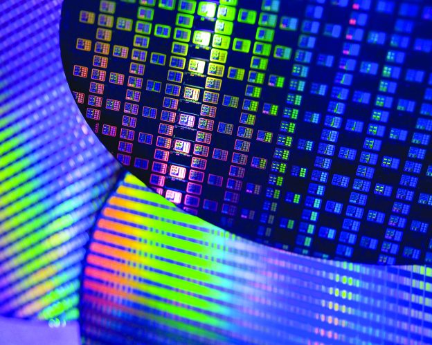
(Image: TSMC)


