Popular Keywords


Intel
News

[News] Musk’s TeraFab Lands First Major Hire as 18-Year Intel Veteran With 18A Experience Joins as Director
Elon Musk's Terafab project has added an Intel veteran to its leadership team. According to Wccftech, Gary Jiang is Tesla's first major hire for the initiative. Jiang announced the move on his LinkedIn profile, where he lists his new role as Director, Tera Fab, a position he assumed in June 2026 and...
News
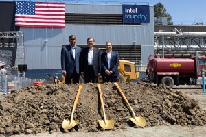
[News] Intel Reportedly Breaks Ground on Santa Clara Expansion for Next-Gen EUV Mask Capacity
As interest in Intel’s foundry services continues to grow among a broader range of tech giants like Apple and NVIDIA, the chipmaker is accelerating its U.S. manufacturing buildout. According to Wccftech, Intel has officially broken ground on the latest expansion of its Santa Clara, California camp...
News
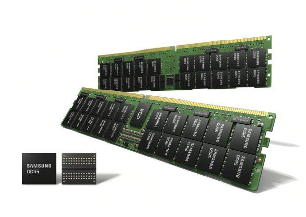
[News] Samsung Reportedly Restarts 1.4nm Push, Targets 2029 Mass Production to Close Gap with TSMC, Intel
As Intel and TSMC both target 1.4nm mass production around 2028-29, Samsung—after reportedly delaying its own roadmap—is now re-entering the race. According to The Bell, the company has resumed efforts to commercialize its 1.4nm (SF1.4) foundry process, with mass production now slated for 2029, ...
News

[News] Samsung, SK hynix 800 Trillion Won Expansion Strains Chipmaking Tool Supply, Potentially Pressures TSMC, Intel
The global semiconductor industry is set to enter a new Warring States era, as Samsung Electronics and SK hynix unveiled a sweeping investment push in South Korea. According to The Elec, the two memory giants will jointly deploy 800 trillion won to build four new fabs in the country’s southwest, a...
News

[News] Intel Taps SK hynix Ex-CEO as Foundry EVP to Lead Advanced Packaging Push as EMIB, HBI Scale Up
Intel CEO Lip-Bu Tan is accelerating the company's foundry ambitions, continuing to recruit seasoned talent from across the chip industry. The latest move is the appointment of Seok-Hee Lee as Executive Vice President of Intel Foundry, according to an Intel announcement on June 18. Notably, Lee j...
- Page 1
- 104 page(s)
- 517 result(s)