Popular Keywords


Intel
News

[News] Decoding Impact: Asia Chipmakers Move to Tackle Helium Strain as Intel Gains Relative Buffer
While Iran and the U.S. have agreed to a ceasefire contingent on guaranteed safe passage through the Strait of Hormuz, the helium crisis across the semiconductor supply chain shows temporary signs of easing. However, as highlighted by Forbes, Qatar’s Ras Laffan Industrial City, which supplies r...
News

[News] Intel Joins Tesla TeraFab, May Provide Design and Manufacturing Strength, Signaling Foundry Momentum
Intel is stepping into Elon Musk’s TeraFab initiative to help to produce 1 TW/year of compute. According to Tom’s Hardware, the company said Tuesday that it is now part of the project, a move that highlights Intel’s ability to design, manufacture, and package advanced processors at scale, pote...
News
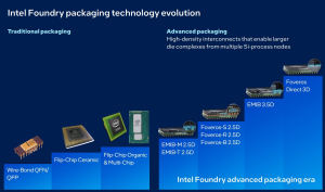
[News] Intel Advanced Packaging Reportedly Gains Traction vs. TSMC as Google, Amazon Weigh EMIB Adoption
Intel’s advanced packaging business is reportedly gaining momentum. According to Wccftech, citing WIRED, sources say the company has been in discussions with at least two major customers—Google and Amazon—on packaging services for ASIC development. This suggests both Google’s TPUs and Amazon...
News

[News] Intel Moves to Reclaim Ireland Fab From Apollo in $14.2B Buyback Amid CPU Demand Strength
Backed by support from the U.S. government and major chip players including NVIDIA, Intel is stepping up efforts to revive its manufacturing strategy amid resilient CPU demand. As it now positions its 18A node for potential external customers, the company is also reclaiming full ownership of its Ire...
News

[News] STMicroelectronics Reportedly to Raise Prices from Apr. 26; Intel, AMD Said to Plan CPU Hikes of 10–15%
Please note that this article cites information from ijiwei, Nikkei, and TechNews. Following the memory price surge, price hikes are now spreading to the analog chip segment. According to ijiwei, sources say STMicroelectronics has sent a price increase letter to customers, stating that prices ac...
- Page 2
- 95 page(s)
- 471 result(s)