[News] Intense Competition with Samsung and Intel in Advanced Processes; TSMC Speeds Up 2nm Progress

The global foundry advanced process battle is reigniting, as reported by the Commercial Times. TSMC’s 2-nanometer process at the Baoshan P1 wafer fab in Hsinchu is set to commence equipment installation as early as April, incorporating a new Gate-All-Around (GAA) transistor architecture and aiming for mass production in 2025.
Additionally, expansion plans for Baoshan P2 and the Kaohsiung fab are projected to join in 2025, with evaluations underway for Phase 2 in the Central Taiwan Science Park. The competition with Samsung and Intel in the most advanced process is intensifying.
Semiconductor industry sources note the ongoing progress in global foundry advanced processes, with Samsung entering GAA architecture early at 3 nanometers, though facing yield challenges, while Intel anticipates mass production of its RibbonFET architecture at 20A this year.
In response to fierce competition, TSMC must accelerate its pace. The ‘Gate-All-Around’ (GAA) technology is a critical factor determining whether chip processing power will double within 1.5 to 2 years.
As per the report, Samsung’s attempt to lead in the 3-nanometer chip segment, transitioning from traditional FinFET, has faced stability issues in yield, hampering customer adoption, and giving TSMC confidence in its 3-nanometer progress. This also highlights the increased complexity in transitioning from 2D to 3D chip designs with GAA transistor architecture.
Furthermore, Intel is intensifying its efforts to catch up, planning to launch Intel 20A in the first half of the year and Intel 18A in the second half. However, it is speculated that Intel 20A will be exclusively used for Intel’s own products, maintaining a close collaboration with TSMC.
TSMC, adopting a cautious approach, benefits from a more advantageous cost structure by minimizing changes in production tools within the same process technology and manufacturing flow. For customers, altering designs during advanced process development incurs significant time and economic costs.
Supply chain sources reveal that TSMC finalized various parameters for its 2-nanometer process at the end of last year, confirming specialty gases and equipment. Contracts are gradually being signed, with equipment installation at the Baoshan P1 fab scheduled to commence in April. Equipment industry sources suggest that TSMC’s process advancement is progressing rapidly as expected, speculating that there will be updates on the Baoshan P2 fab later this year.
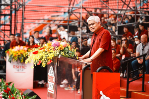
(Image: TSMC)


