Popular Keywords


2nm
News

[News] Chinese Startup Dishan Reportedly Develops 2nm AI Chip in Prototype Verification; Foundry Access Uncertain
China may be on the verge of another advanced chip breakthrough. According to South China Morning Post, citing local outlets icrank and Shanghai Morning Post, sources say Chinese startup Dishan Technology has made progress in developing a 2nm AI chip. The company is currently in the prototype verifi...
News

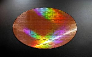
[News] Samsung 2nm Yields Reportedly at ~55%, Below Mass Production Threshold; Qualcomm May Opt for TSMC
Samsung’s 2nm yield challenges are resurfacing. According to Busan Ilbo, sources indicate that Samsung Foundry’s 2nm yields remain in the mid-50% range, falling short of the roughly 60% threshold typically required for stable mass production. After backend processing, effective yields are expec...
News

[News] Delay at Samsung’s Taylor Reportedly Slips Mass Production to 2027, Raising Concerns for Tesla
As Samsung accelerates fab approvals and equipment installations, questions are emerging about the pace of mass production at the Taylor plant. Korea JoongAng Daily reports that the start of full-scale production at Samsung’s Texas facility is now expected to slip to early 2027. If confirmed, t...
News

[News] TSMC Speeds up Expansion in Taiwan: up to 10 Fabs Reportedly under Construction or Starting in 2026
As NVIDIA is scheduled to release its Q1 earnings release on February 25 and the GTC 2026 conference in March, major foundry partner TSMC’s expansion move keeps drawing market attention. Liberty Times, citing semiconductor supply chain sources, reports TSMC could have up to 10 fabs across Taiwan�...
News
[News] Japan’s Chip Push in Spotlight: IBM Backs Rapidus as Funding Momentum Builds
As TSMC upgrades its second Kumamoto fab to 3nm, Japan’s homegrown foundry Rapidus is also drawing market attention. Hokkaido Shimbun reports IBM is backing the effort, planning a new office in downtown Chitose this spring to support Rapidus’ next-gen chip ambitions. IBM maintains a close par...
- Page 1
- 26 page(s)
- 127 result(s)