Popular Keywords


2nm
News

[News] India’s Chip Ambitions Grow: Qualcomm Completes 2nm Tape-Out, MediaTek Reportedly Mulls Entry
As India ramps up its semiconductor push, smartphone chip giant Qualcomm has completed the tape-out of a 2nm chip design in the country, marking a major milestone, according to local media Business Standard. The report, citing Qualcomm, notes that the work was carried out across the company’s e...
News
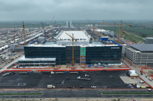
[News] Samsung Reportedly Secures Partial Taylor Fab Use Approval, Timeline May Move Up
Samsung’ Taylor fab is reportedly making tangible progress. Citing Korea JoongAng Daily, the report says the company has obtained temporary approval for portions of its facility under construction in Taylor, potentially accelerating the project from its original schedule. As noted in the report...
News

[News] TSMC 2nm Reportedly Tight Amid Mobile, HPC Demand; NVIDIA May Be First to Adopt 1.6nm in 2028
NVIDIA CEO Jensen Huang hosted a dinner on the evening of the 31st for senior executives from key supply-chain partners. As noted by Economic Daily News, Huang said TSMC must work at full stretch this year, underscoring tight capacity for its advanced nodes. TSMC’s 2nm capacity has reportedly been...
News
[News] Samsung Foundry Reportedly Expects 30%+ 2nm Order Growth in 2026; 1.4nm Set for 2029
Samsung appears to be gaining momentum in advanced processes, with signs of a potential rebound in its foundry business. According to ZDNet, Samsung Electronics said progress on its 2nm node, along with related customer order intake, is proceeding smoothly. The report notes that the company says th...
News
[News] Samsung Reportedly Sets March EUV Trials at Taylor Fab Ahead of Tesla Chip Production
While TSMC signals plans to accelerate its Arizona expansion amid rumors of five additional fabs, Samsung is also pushing ahead at its Taylor site. According to Hankyung, trial operations of extreme ultraviolet (EUV) lithography equipment at Taylor Fab 1 will start this March, setting the stage for ...
- Page 2
- 26 page(s)
- 127 result(s)