Popular Keywords


2nm
News

[News] TSMC Earnings Preview: $150B Capex Over Next Three Years Tops Five Key Focuses
Ahead of TSMC’s earnings call on January 15, the market has already been flooded with reports that the company may build five additional fabs in Arizona under a U.S.–Taiwan trade framework. But what else should investors be watching when results are released tomorrow? A TechNews report flags ...
News
[News] TSMC Reportedly Suspends New 3nm Kick-offs, Steers Customers to 2nm to Optimize Costs
TSMC recently announced the successful mass production of its 2nm process, while industry rumors suggest the company has put new 3nm projects on hold. According to Commercial Times, sources indicate that TSMC has not only raised prices for its 3nm process this year, but has also temporarily suspend...
News

[News] Earnings Call Preview: TSMC 2nm in Focus — Capacity, Sales Contribution, and More
Ahead of TSMC’s earnings call on January 15, the company quietly confirmed that its 2nm process entered mass production on schedule in 4Q25. With the market now expecting more details at the briefing, here are some of the key things to watch as this long-anticipated node steps into the spotlight. ...
News

[News] Samsung Set to Benefit from TSMC’s ‘N-2’ Rule as AMD, Google Eye U.S. 2nm Production
As TSMC ramps up its U.S. and Japan expansions, all eyes are on the so-called “N-2” rule, which, according to the Central News Agency, could prevent the foundry giant from producing its most advanced nodes overseas. South Korean media outlet ebn reports that Samsung is set to capitalize on this ...
News
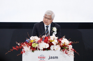
[News] TSMC’s Bold Pivot: Kumamoto Fab 2 Reportedly Leaps from 6nm to 2nm amid JASM Losses
While TSMC’s Arizona expansion races ahead, its Japan operations are moving at a slower pace, drawing close attention. Plans for Kumamoto Fab 2, however, may be shifting. A Nikkei report had suggested a move to 4nm—originally planned for 6nm and 7nm—but Mirror Media now reports a bolder plan: ...
- Page 3
- 26 page(s)
- 127 result(s)