TSMC


2024-02-07

[News] US Allocates USD 39 Billion Subsidy to Semiconductor Industry for Establishing Plants

US Commerce Secretary Gina Raimondo has announced on February 5th that the Commerce Department would distribute substantial subsidies to chipmakers investing in the US within the next two months. The subsidy recipients are expected to include companies like TSMC and Intel.

As per a report from Reuters, Raimondo discussed the progress of subsidies under the US CHIPS and Science Act. “We’re in the process of really complicated, challenging negotiations with these companies. In the next six to eight weeks, you will see several more announcements. That’s what we’re striving for,” she stated.

Raimondo did not specify which chipmakers she is negotiating with, but she mentioned in an interview cited by Reuters,”These are highly complex, first-of-their-kind facilities. The kind of facilities that TSMC, Samsung, Intel are proposing to do in the United States — these are new-generation investments — size, scale complexity that’s never been done before in this country.”

Last month, as per Bloomberg cited industry sources in a report, plans for the United States to announce substantial chip subsidies by the end of March are revealed, targeting companies such as TSMC and Intel. The US CHIPS and Science Act reportedly includes a USD 39 billion manufacturing subsidy, providing 15% of the total cost for each independent project. Each fab can receive up to USD 3 billion in subsidies, along with loans, loan guarantees, and tax exemptions.


Read more

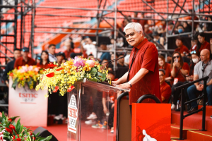
(Photo credit: TSMC)

Please note that this article cites information from ReutersBloomberg.

2024-02-07

[News] TSMC’s JASM Kumamoto Plant 2 Greenlit, Construction Expected to Commence by Year’s End

TSMC officially gives the green light to the second fab in Kumamoto, Japan! On January 6th, TSMC, Sony Semiconductor Solutions Corporation (SSS), DENSO Corporation (DENSO), and Toyota Motor Corporation (Toyota) jointly announced further investment in TSMC’s Japanese subsidiary, Japan Advanced Semiconductor Manufacturing, Inc. (JASM).


The collaboration is expected to construct JASM’s second fab in Japan, dedicated to the 6/7-nanometer advanced process. The new facility is expected to commence operations by the end of 2027, with a total investment exceeding USD 20 billion, strongly supported by the Japanese government.

TSMC has stated that in this investment venture with JASM, TSMC, SSS, DENSO, and Toyota hold approximately 86.5%, 6.0%, 5.5%, and 2.0% of JASM shares, respectively. Toyota Motor Corporation is a new major shareholder following this capital increase, indicating its potential involvement in automotive electronics initiatives.

TSMC has further indicated that the construction of JASM’s second fab in Japan is set to commence at the end of 2024. The expansion in production capacity is expected to optimize overall cost structure and supply chain efficiency.

With two fabs in Kumamoto, TSMC anticipates in the press release that JASM’s total monthly production capacity will exceed 100,000 12-inch wafers, offering process technologies ranging from 40nm, 22/28nm, 12/16nm, to 6/7nm for automotive, industrial, consumer, and high-performance computing (HPC) applications. Capacity planning may be further adjusted based on customer demand.

For JASM’s first fab, it is planned to commence production by the end of the year. The initial facility, costing USD 8.6 billion, received subsidies of JPY 478 billion (approximately USD 3.23 billion) from the Japanese government.

The primary process of the first fab are 22/28nm and 12/16nm, with a monthly production capacity of around 50,000 12-inch wafers. Located in Kikuyo-cho, Kikuyo-gun, Kumamoto Prefecture, Kyushu, construction of the facility was announced in November 2021, ground was broken in April 2022, and construction was completed within two years.

JASM’s first fab is set to open on February 24, 2024, with mass production scheduled by the end of the year. The facility is a joint venture between Taiwan and Japan, with TSMC holding the majority of shares, Sony Semiconductor Manufacturing Corporation (SSMC) of Japan holding approximately 20%, and Toyota Group’s DENSO holding about 10%.

Read more

2024-02-07

[Insights] OpenAI CEO’s Ambition to Build Semiconductor Plant Grows Stronger

In late December 2023, reports surfaced indicating OpenAI CEO Sam Altman’s intention to raise funds to construct a semiconductor plant, ensuring a secure supply of AI chips.

According to a report from the Washington Post on January 24, 2024, Sam Altman has engaged with US congressional members to discuss the construction of the semiconductor plant, including considerations of timing and location, highlighting his increasingly fervent ambition to establish the facility.

TrendForce’s Insights:

  • Rising AI Computing Demands Heighten Sam Altman’s Concerns About Chip Supply

The rapid emergence of AI-generated content (AIGC) undoubtedly stood out as a highlight of 2023, closely tied to the quality and efficiency of the large language models (LLMs) used. Take OpenAI’s ChatGPT, for instance, which employs the GPT-3.5 model released in 2020. With 175 billion training parameters, it surpasses its predecessor, GPT-2, by over 100 times, itself being over 10 times larger than the initial GPT from 2018.

In pursuit of better content quality, diversified outputs, and enhanced efficiency, the continuous expansion of model training parameters becomes an inevitable trend. While efforts are made to develop lightweight versions of language models for terminal devices, the cloud-based AI computing arena anticipates a continued expansion of language model training parameters, moving towards the “trillion” scale.

Due to the limited growth rate of AI chip performance, coping with the rapidly increasing model training parameters and the vast amount of data generated by the flourishing development of cloud-based AIGC applications inevitably requires relying on more AI chips. This situation continues to exert pressure on the chip supply chain.

Given that the demand for AI computing is escalating faster than the growth rate of chip performance and capacity, it’s understandable why Sam Altman is concerned about chip supply.

  • Sam Altman to Seek Collaboration with Foundries for Plant Construction Goal

The construction of advanced process fabs is immensely costly, with estimates suggesting that the construction cost of a single 3nm fab could amount to billions of dollars. Even if Sam Altman manages to raise sufficient funds for plant construction, there remains a lack of advanced semiconductor process and packaging technology, not to mention capacity, yield, and operational efficiency.

Therefore, it is anticipated that Sam Altman will continue to seek collaboration with sfoundries to achieve his factory construction goal.

Looking at foundries worldwide, TSMC is undoubtedly the preferred partner. After all, TSMC not only holds a leading position in advanced processes and packaging technologies but also boasts the most extensive experience in producing customized AI chips.

While Samsung and Intel are also suitable partners from a localization perspective, considering factors like production schedules and yield rates, choosing TSMC appears to be more cost-effective.

(Photo credit: OpenAI)

Please note that this article cites information from The Washington Post.

2024-02-06

[News] Samsung Accelerates 3D Packaging with Hybrid Bonding Production Line in Korean Advanced Packaging Hub

In a bid to enhance its foundry capabilities, Samsung is earnestly integrating hybrid bonding technology. According to industry sources, Applied Materials and Besi Semiconductor are establishing equipment for hybrid bonding at the Cheonan Campus, slated for use in next-generation packaging solutions like X-Cube and SAINT.

According to a report from South Korean media outlet The Elec, industry sources have indicated that Applied Materials and Besi Semiconductor are installing hybrid bonding equipment at Samsung’s Cheonan Campus, a key site for advanced packaging production. Officials from the South Korean industry also mentioned that a production line is currently under construction, with the equipment intended for non-memory packaging.

Compared to existing bonding methods, hybrid bonding enhances I/O and wiring lengths. Samsung’s latest investment is expected to strengthen its advanced packaging capabilities, introducing the X-Cube utilizing hybrid bonding technology.

Industry sources cited by the report have suggested that hybrid bonding could also be applied to Samsung’s SAINT (Samsung Advanced Interconnect Technology) platform, which the company began introducing this year. The platform includes three types of 3D stacking technologies: SAINT S, SAINT L, and SAINT D.

SAINT S involves vertically stacking SRAM on logic chips such as CPUs. SAINT L involves stacking logic chips on top of other logic chips or application processors (APs). SAINT D entails vertical stacking of DRAM with logic chips like CPUs and GPUs.

TSMC, the leading semiconductor foundry, also offers hybrid bonding in its System on Integrated Chip (SoIC) for 3D packaging services, which is similarly provided by Applied Materials and Besi Semiconductor. Intel has also applied hybrid bonding technology in its 3D packaging technology, Foveros Direct, which was commercialized last year.

Reportedly, industry sources anticipate that Samsung’s investment in hybrid bonding facilities is poised to attract major clients such as NVIDIA and AMD. This is because the demand for hybrid bonding among fabless customers is steadily increasing.

(Photo credit: Samsung)

Please note that this article cites information from The Elec.

2024-02-01

[News] Intensified Competition in the Semiconductor Industry for 2nm Technology Dominance, Potentially Reshaping the Global Foundry Market

The competition for dominance in 2nm semiconductor technology has intensified at the beginning of 2024, marking a crucial battleground among global foundry companies.

As per a report from IJIWEI, major foundry enterprises such as Samsung Electronics, TSMC, and Intel are set to commence mass production adopting 2nm process starting this year. Consequently, the fierce competition for supremacy in 2nm technology is expected to escalate from 2025 onwards. Currently, the most advanced production technology globally is at the 3nm level.

  • TSMC

TSMC’s 2nm products will be manufactured at the Fab 20 in the Hsinchu Science Park in northern Taiwan and at a plant in Kaohsiung.

The Fab 20 facility is expected to begin receiving related equipment for 2nm production as early as April, with plans to transition to GAA (Gate-All-Around) technology from FinFET for 2nm mass production by 2025.

During TSMC’s earnings call on January 18th, TSMC revealed that its capital expenditure for this year is expected to fall between USD 28 billion and 32 billion, with the majority (70% to 80%) allocated to advanced processes. This figure is similar to that of 2023 (USD 30.4 billion), indicating stable investment to ensure its leading position in 2nm technology.

  • Intel

After announcing its re-entry into the foundry business, Intel is actively advancing its foundry construction efforts. The plan includes the introduction of the Intel 20A (equivalent to 2nm) process in the first half of 2024 and the Intel 18A (1.8nm) process in the second half of the year. It is understood that the Intel 18A process will commence test production as early as the first quarter of this year.

Intel’s 2nm roadmap is more ambitious than originally anticipated, being accelerated by over six months. In response to criticisms of its “overly ambitious” plans, Intel swiftly began procuring advanced Extreme Ultraviolet (EUV) equipment.

  • Samsung Electronics

Samsung Electronics has devised a strategy to gain an advantage in the more advanced process war through its Gate-All-Around (GAA) technology. Currently, it is mass-producing the first-generation 3nm process based on GAA (SF3E) and plans to commence mass production of the second-generation 3nm process this year, significantly enhancing performance and power efficiency.

Regarding the 2nm process, per a report from Nikkei, Samsung plans to start mass production for mobile devices in 2025 (SF2) and gradually expand to high-performance computing (HPC) in 2026 and automotive processes in 2027.

Currently, Samsung Electronics is producing GAA products for the 3nm process at its Hwaseong plant and plans to manufacture products for both the 3nm and 2nm processes at its Pyeongtaek facility in the future.

  • Rapidus

Rapidus, a chip manufacturing company supported by the Japanese government, is expected to trial-adopt 2nm process at its new plant by 2025 and begin mass production from 2027.

If Rapidus’ technology is validated, the global foundry market may expand beyond the Taiwan-Korea duopoly to include Taiwan, Korea, the United States, and Japan.

The technology competition to become a “game-changer” ultimately depends on the competition for customers. It’s rumored that TSMC holds a leading position in the 2nm field, with Apple speculated to be its first customer for the 2nm process. Graphics processing giant NVIDIA is also considered a major customer within TSMC’s client base.

According to TrendForce data as of the third quarter of 2023, TSMC’s revenue share accounted for a dominant 57.9%, with Samsung Electronics trailing at 12.4%, a gap of 45.5 percentage points.

However, Samsung Electronics is not sitting idly by. With continuous technological investment, Samsung’s foundry customer base grew to over 100 in 2022, a 2.4-fold increase from 2017. The company aims to expand this number to around 200 by 2028.

Particularly, Samsung’s early adoption of GAA technology is expected to give it an advantage in achieving early production volumes for advanced processes.

Read more

(Photo credit: TSMC)

Please note that this article cites information from IJIWEI and Nikkei.

  • Page 1
  • 45 page(s)
  • 224 result(s)