Popular Keywords


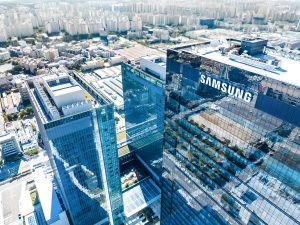
Samsung
News

[News] TSMC on Terafab: No Shortcuts in Foundry; Reportedly Confirms Next-Gen NVIDIA LPU Project amid Samsung Rivalry
With Tesla teaming up with Intel on the “Terafab” initiative and accelerating its push into chip manufacturing, attention in the market is turning to how TSMC will respond. At today’s earnings call, chairman C.C. Wei acknowledged that both Intel and Tesla remain TSMC customers, while also call...
News
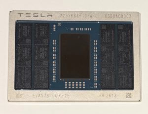
[News] Tesla AI5 Reportedly Uses SK hynix Memory, Samsung LPDDR5X; Samsung SF2T Process Applied Ahead of AI6
Tesla has announced that its AI5 chip has officially completed tape-out, with additional details now emerging. According to Hankyung, the prototype has been confirmed to be produced on Samsung Electronics’ domestic foundry line. As highlighted by SEDaily, the marking “KR2613” is visible on the...
News
[News] Musk Confirms AI5 Tape-Out, but Wrong TSMC Tag Triggers Social Media Mix-Up
While Tesla is collaborating with Intel on its ambitious Terafab project, the company has also reached a key milestone in its next-generation AI chip program. According to Tesla CEO Elon Musk on X, the AI5 chip has officially completed tape-out. As previously reported by TechPowerUp, Tesla opts t...
News
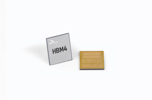
[News] HBM4 Strategies Diverge: Samsung Reportedly Chases 80% 1c DRAM Yield While SK hynix Trims Shipments by 30%
As memory giants enter the final stage of HBM4 ramp-up ahead of NVIDIA’s Rubin launch, they are taking diverging approaches. According to Chosun Biz, Samsung is pushing to lift 1c DRAM yields for HBM4 toward 80%, while ZDNet reports that SK hynix is set to cut HBM4 volumes this year by 20–30%. ...
News
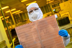
[News] Korea Challenges Intel on Glass Substrate Standards as Absolics, Samsung Accelerate Commercialization
Commercialization of glass substrates is accelerating, with South Korean players and Intel increasingly competing head-on for leadership. According to Global Economic, sources indicate that Intel has laid out a glass substrate roadmap targeting 2030 to secure a technological edge, while Korean firms...
- Page 1
- 165 page(s)
- 825 result(s)