Popular Keywords


Samsung
News
[News] Samsung 2nm Yields Reportedly at ~55%, Below Mass Production Threshold; Qualcomm May Opt for TSMC
Samsung’s 2nm yield challenges are resurfacing. According to Busan Ilbo, sources indicate that Samsung Foundry’s 2nm yields remain in the mid-50% range, falling short of the roughly 60% threshold typically required for stable mass production. After backend processing, effective yields are expec...
News
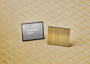
[News] Samsung Reportedly Lifts HBM4 Logic Die Prices by 40–50% Amid AI Boom; 4nm at Full Capacity
Memory is not the only segment where Samsung Electronics is pushing price increases amid surging AI demand. According to Financial News, the chip giant has reportedly raised prices for HBM4 logic dies by around 40–50% since early 2026, signaling a broader normalization of pricing across its semico...
News
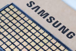
[News] Samsung-Backed Vertical Die Research Reportedly Targets 10x I/O and 4x Bandwidth Gains for HBM
Although JEDEC is expected to ease height restrictions for HBM, raising the limit to around 900 micrometers (µm) from 775 µm in HBM4, the industry continues to search for ways to overcome the structural limits of conventional HBM architectures. According to ET News, a “Vertical Die”-based adva...
News

[News] Samsung Reportedly Bets on Vietnam with $4B Chip Packaging Push; Amkor Expands Presence
Semiconductor giants are accelerating global advanced packaging expansion as demand for AI chips surges, with Southeast Asia emerging as one of the most sought-after hubs. While Intel is set to bring its advanced packaging facility in Malaysia online later this year, Bloomberg reports that Samsung i...
News
[News] Samsung Reportedly Tops 2,000 Patent Approvals in China in Q1 as AI Memory and Advanced Chips Drive Surge
While the rapid rise of China’s semiconductor players has fueled debate over whether the technological gap with industry leaders is narrowing, Samsung is signaling its own offensive by accelerating its patent push in the region. According to The Guru, Samsung sharply increased patent approvals in ...
- Page 2
- 165 page(s)
- 825 result(s)