[News] Intel Secures First High-NA EUV Equipment, Threatening TSMC’s Position?
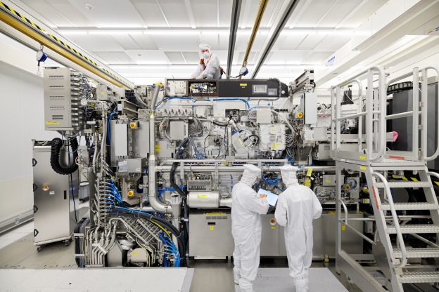
Intel recently announced that it has acquired the market’s first ASML Extreme Ultraviolet (EUV) exposure equipment with a 0.55 Numerical Aperture (High-NA), aiming to advance its chip manufacturing technology in the coming years. In contrast, TSMC appears to be taking a more cautious approach, currently showing no urgency to join the race for this next-generation exposure technology.
The High-NA EUV exposure equipment obtained by Intel will initially be used for learning and mastering the technology, with plans to implement it in the Intel 18A process node in the next two to three years.
Industry sources suggest that unlike Intel’s plan to introduce High-NA EUV and GAA transistors simultaneously in the Intel 18A process technology, it is anticipated that TSMC may not adopt this technology until the 1.4nm (A14) node, possibly in 2030 or later.
According to a report from IThome, in fact, Intel’s proactive development roadmap includes implementing the RibbonFET gate-all-around (GAA) transistor architecture and PowerVia backside power delivery technology starting from the Intel 20A process.
Subsequently, further optimizations are expected in the Intel 18A process, followed by the adoption of High-NA EUV exposure equipment in subsequent process nodes after Intel 18A. These advancements is anticipated to achieve lower power consumption, higher performance, and smaller chip sizes.

In addition, Intel plans to introduce pattern shaping starting from the 20A process, followed by the adoption of High-NA EUV after the 18A node. This approach is expected to reduce the complexity of the manufacturing process and avoid the use of EUV double patterning.
However, some professionals in the industry have stated that, at least in the initial stages, the cost of High-NA EUV may be higher than that of Low-NA EUV. Furthermore, High-NA EUV lithography equipment present a series of specific challenges too, including a halving of the exposure area.
These are two of the reasons why TSMC is currently adopting a cautious approach. TSMC tends to favor the use of cost-effective mature technologies to ensure product competitiveness.
In fact, If we look back at the development of EUV technology, TSMC began using EUV exposure equipment in chip production as early as 2019, a few months later than Samsung but several years ahead of Intel. Currently, Intel is expected to take the lead in the High-NA EUV field ahead of Samsung and TSMC to gain a certain technological and strategic advantage, increasing its appeal to customers.
Therefore, whether TSMC can maintain its leading position in process technology, especially if it adopts High-NA EUV exposure machines later than competitors, remains subject to ongoing observation.
Read more
- [News] EUV as a Strategic Asset in the Most Advanced Processes: Progress in Intel/TSMC/Samsung’s Adoptions
- [Insights] Analysis of the Global Photoresist Market in 2023
(Photo credit: ASML)
Please note that this article cites information from IThome


