Popular Keywords


EUV
News
[News] ASML Raises 2026 Sales Outlook to €36B–€40B on Memory, Logic Demand; South Korea Share Hits 45%
Amid an AI-driven capex upcycle among memory and logic customers, ASML has raised its 2026 revenue outlook. The Dutch chipmaking tool giant now expects sales to reach €36 billion to €40 billion (US$42–47 billion), up from its previous forecast of €34 billion to €39 billion, with a gross ma...
News
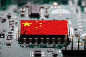
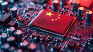
[News] U.S. Proposes to Tighten China Chip Tool Exports; Targets DUV to Slow SMIC and Peers’ Advanced Node Push
The U.S. is reportedly advancing a bill to further tighten China’s access to chipmaking equipment. According to South China Morning Post, U.S. lawmakers have proposed the Multilateral Alignment of Technology Controls in Hardware (MATCH) Act, which aims to close “critical gaps” in existing res...
News
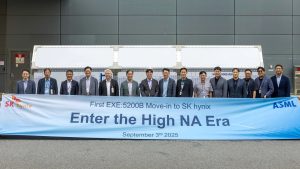
[News] SK hynix Commits $8B to ASML EUV Equipment by 2027 in Push for AI Memory Dominance
Please note that this article cites information from Yonhap News, Reuters, The Chosun Daily, The Dong‑A Ilbo, ET News and SK hynix. SK hynix is moving aggressively to expand its AI memory capabilities, reportedly planning a U.S. ADR listing to fuel growth, while already securing critical chipma...
News
[News] Iran Conflict Threatens Helium for Chip: China’s Domestic Supply Push in Focus
The Iran conflict is raising concerns over the supply of key semiconductor materials. As noted by Nikkei, Middle East crisis is casting a shadow over Asia’s chip supply chain as fears grow that the de facto closure of the Strait of Hormuz could persist. Seoul is particularly concerned about helium...
News
[News] “China’s ASML” by 2030? SMIC, Naura and Other Chip Leaders Call for National Effort
China has been accelerating its push for semiconductor self-reliance amid U.S. restrictions, and a new article written by the country’s leading chip executives has outlined a strategic roadmap. According to South China Morning Post, top figures in China’s semiconductor industry co-authored the p...
- Page 1
- 20 page(s)
- 96 result(s)