Popular Keywords


IC Manufacturing, Package&Test
News
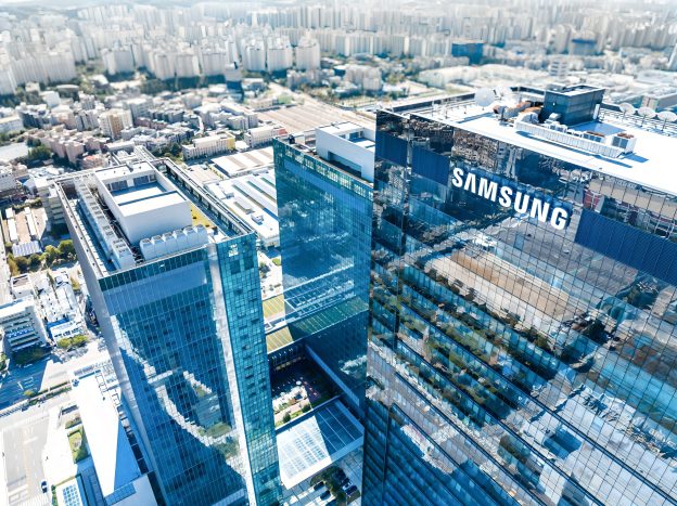
[News] TSMC, Samsung Reportedly Cut 8-Inch Wafer Output, Boosting Korea’s DB HiTek
Samsung and TSMC are reportedly scaling back their 200mm (8-inch) foundry operations in response to shifting industry dynamics. According to South Korean outlet Hankyung, the two chipmakers have recently begun focusing more on advanced manufacturing using 300mm (12-inch) wafers to produce high value...
News

[News] GlobalFoundries Licenses TSMC’s 650V, 80V GaN Tech in Sign of Foundry Leader’s Retreat
In line with its strategy to focus on advanced chip technologies, TSMC is gradually retreating from lower-margin mature technology segments. Reflecting this shift, GlobalFoundries announced on November 10 a technology licensing deal with TSMC for 650V and 80V Gallium Nitride (GaN) technologies. Acco...
News

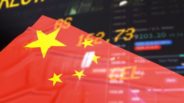
[News] Decoding China’s Lithography Push to Challenge ASML: From SiCarrier to Alternative EUV Paths
As Bejing advances toward semiconductor self-reliance, high-end chipmaking tools are indispensable—yet lithography, controlled by ASML, poses the biggest challenge, with its EUV machines for sub-5nm chips off-limits for export. Notably, 42% of ASML’s Q3 2025 sales came from China, underscoring t...
News
[News] ASML’s Magic Uncovered: Tech and Partners Behind Its EUV Edge China Can’t Replicate
While China is racing to close the lithography gap with homegrown tools from Huawei-linked SiCarrier and Yuliangsheng, the reality is that extreme ultraviolet (EUV) lithography remains an entirely different universe. Machines capable of printing sub-5nm chips are not just complex—they’re the pin...
News
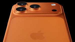
[News] TSMC Reportedly Notifies Clients of 8–10% Sub-5nm Hike in 2026, Apple A- & M-Chips Affected
Amid growing speculation that TSMC has begun alerting clients to a 2026 price hike, new reports are adding fuel to the fire. According to a Naver post by leaker yeux1122, cited by MacRumors and Wccftech, the foundry giant has notified key customers—including Apple—of upcoming price increases for...
- Page 30
- 179 page(s)
- 895 result(s)