Popular Keywords

IC Manufacturing, Package&Test
News
[News] TSMC’s CoWoS-L/ S Reportedly Fully Booked, OSAT Partners Step up with ASE’s CoWoP in Focus
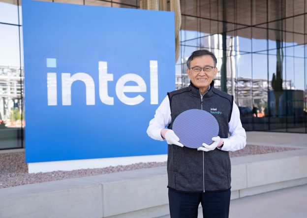
Amid heightened attention on Intel’s EMIB (Embedded Multi-die Interconnect Bridge), TSMC is experiencing exceptionally strong demand for its own advanced packaging. According to Economic Daily News, a surge of AI and HPC orders from NVIDIA, Google, Amazon, and MediaTek has driven TSMC’s entire C...
News

[News] Tokyo Electron Sees AI-Driven Sales Hitting 40% by FY2026, Offsetting China Slowdown
U.S. export controls are hitting global chip-tool makers, and Tokyo Electron (TEL) is scrambling to make up for shrinking orders from China. According to a recent interview with Nikkei, Executive Managing Director for finance Hiroshi Kawamoto says that by fiscal 2026, the company’s equipment for a...
News
[News] Inside Huawei’s Patent Playbook: GPU Dominance and Sub-2nm Ambitions Under Sanctions
As China accelerates its push for semiconductor self-sufficiency, all eyes are on how leading tech firms are advancing cutting-edge technologies under U.S. sanctions, with Huawei clearly at the forefront. According to Nikkei, the Chinese chip giant has dramatically ramped up GPU-related patent filin...
News

[News] Intel Eyes EMIB to Ramp up in 2H26; 18A‑P/18A‑PT Moves Toward External Adoption
As interest around Intel’s EMIB (Embedded Multi-die Interconnect Bridge) continues to build—including reports linking it to a Google-MediaTek TPU—the industry is watching closely for signs of a real ramp. According to Intel’s Corporate Vice President John Pitzer, the technology is expected t...
News
[News] Chinese Semiconductor Equipment Maker PSR Completed Series A Funding
Recently, PSR Semi, based in Jiangsu China, announced the successful closing of a Series A funding round worth RMB several hundred million. The round was led by prominent investors including Yongxin Fangzhou, Jinyuan Capital, and Hefei Industry Investment, among others. Headquartered in Wuxi, PSR...
- Page 26
- 181 page(s)
- 905 result(s)