Popular Keywords


IC Manufacturing, Package&Test
News
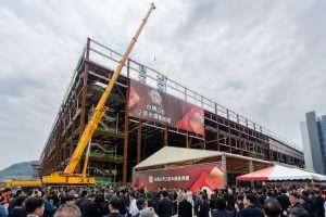
[News] TSMC Reportedly Plans 2-nm Boost in Taiwan with Three New Fabs, NT$900B Investment
Last week, TSMC Chairman C.C. Wei received the semiconductor industry's top honor, the Robert N. Noyce Award, and revealed that demand now exceeds the company’s capacity by three times, leaving advanced process capacity “massively insufficient,” Commercial Times reports. Amid surging AI chip d...
News
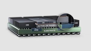
[News] Intel’s EMIB Reportedly Gains Traction with AI ASIC, Smartphone Clients, Could Package TSMC Dies
Recent reports that Apple and Qualcomm are recruiting engineers with EMIB (Embedded Multi-die Interconnect Bridge) expertise suggest Intel’s packaging technology is regaining momentum—helped in part by the tight squeeze on TSMC’s capacity. According to the Commercial Times, the shift indicates...
News

[News] Intel’s Two-Front Push: 18A Yields Reportedly Rise 7% Monthly, 14A Enters Definition Stage
While Intel gears up to unveil its first 18A-based product, Panther Lake, at CES 2026 in early January, the company offered a progress update at this week’s RBC Capital Markets’ tech conference: 18A yields are reportedly climbing 7% per month, and 14A has already entered the definition phase. ...
News
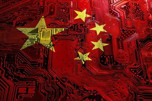
[News] US Lawmakers Could Eye 10-Year Ban on CHIPS Act Grants Buying Chinese Chip Tools, with Waivers
While U.S. officials have reportedly signaled that long-anticipated semiconductor tariffs may not be imposed anytime soon, the country is maintaining strict controls on China’s chip industry. As part of these ongoing efforts, Reuters reports a bipartisan group of U.S. lawmakers on Thursday introdu...
News

[News] Ex-TSMC SVP Wei-Jen Lo Moves to Intel: Sub-2nm Data Leak Concerns and TSMC Strategy in Focus
Fresh off a 2nm data leak involving its engineers in August, TSMC is now facing an even bigger headache: rumors that former Senior VP Wei-Jen Lo—who reportedly joined Intel recently after retiring in July—had subordinates brief him and photocopy sensitive sub-2nm process materials before he left...
- Page 27
- 179 page(s)
- 892 result(s)