Popular Keywords


IC Manufacturing, Package&Test
News
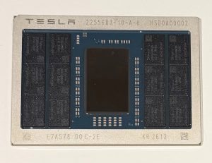
[News] Musk Confirms AI5 Tape-Out, but Wrong TSMC Tag Triggers Social Media Mix-Up
While Tesla is collaborating with Intel on its ambitious Terafab project, the company has also reached a key milestone in its next-generation AI chip program. According to Tesla CEO Elon Musk on X, the AI5 chip has officially completed tape-out. As previously reported by TechPowerUp, Tesla opts t...
News
[News] ASML Raises 2026 Sales Outlook to €36B–€40B on Memory, Logic Demand; South Korea Share Hits 45%
Amid an AI-driven capex upcycle among memory and logic customers, ASML has raised its 2026 revenue outlook. The Dutch chipmaking tool giant now expects sales to reach €36 billion to €40 billion (US$42–47 billion), up from its previous forecast of €34 billion to €39 billion, with a gross ma...
News
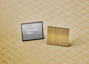
[News] Samsung Reportedly Lifts HBM4 Logic Die Prices by 40–50% Amid AI Boom; 4nm at Full Capacity
Memory is not the only segment where Samsung Electronics is pushing price increases amid surging AI demand. According to Financial News, the chip giant has reportedly raised prices for HBM4 logic dies by around 40–50% since early 2026, signaling a broader normalization of pricing across its semico...
News
[News] Intel Launched World’s First Thinnest GaN Chiplet
On April 9, Intel Foundry Services announced a major technological breakthrough with the development of the world’s thinnest gallium nitride (GaN) chiplet. The silicon substrate has been reduced to just 19 micrometers—approx. one-fifth the diameter of a human hair. The chiplet is fabricated o...
News

[News] TSMC Advances Panel-Level Packaging, CoPoS Pilot Line Reportedly Set for June Completion, 2028–29 Ramp Eyed
Ahead of TSMC’s earnings call later this week, the spotlight is once again on its advanced packaging roadmap—and CoWoS is no longer the only story. According to Commercial Times, TSMC’s CoPoS (Chip-on-Panel-on-Substrate) pilot line has already begun tool deliveries to R&D teams in February...
- Page 2
- 179 page(s)
- 892 result(s)