Popular Keywords


IC Manufacturing, Package&Test
News
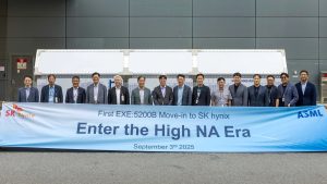
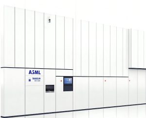
[News] SK hynix Commits $8B to ASML EUV Equipment by 2027 in Push for AI Memory Dominance
Please note that this article cites information from Yonhap News, Reuters, The Chosun Daily, The Dong‑A Ilbo, ET News and SK hynix. SK hynix is moving aggressively to expand its AI memory capabilities, reportedly planning a U.S. ADR listing to fuel growth, while already securing critical chipma...
News
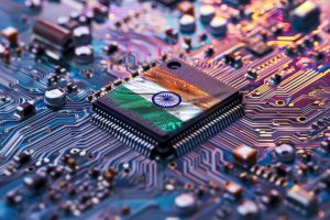
[News] India’s Chip Output Set to Reach 75–80 Million Units per Day, Marking a New Milestone
India’s semiconductor ecosystem is entering a period of significant transformation. According to the India Electronics and Semiconductor Association (IESA) and its president, Ashok Chandak, the country’s chip production capacity could reach 75 million to 80 million units per day by late 2026 or ...
News
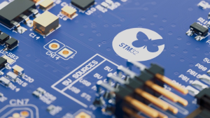
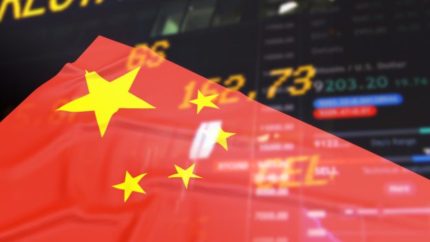
[News] STMicroelectronics Launches Locally Made STM32 MCUs in China via Huahong Partnership
Please note that this article cites information from Reuters, ijiwei, EE News Analog, and STMicroelectronics. STMicroelectronics has taken a major step to meet China’s growing chip demand. Reuters, citing a company press release, reports that the European chipmaker began shipping STM32 wafers t...
News
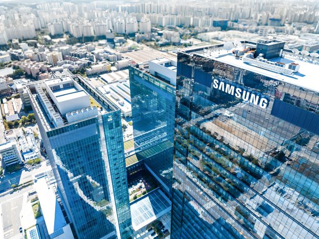
[News] Under Qatar’s Shadow: Helium Crunch Hits South Korea Harder, Putting Samsung, SK hynix, TSMC in Spotlight
Please note that this article cites information from CNBC, Liberty Times, TechNews, Maeil Business, Hankyung and Solution News. The Middle East war, widely known for driving oil prices up, is also threatening the semiconductor industry by hitting a critical yet little-known resource: helium. As r...
News
[News] ASML Reportedly Eyes Hybrid Bonding Equipment, Precision Edge May Reshape Advanced Packaging Landscape
Please note that this article cites information from The Elec. Rumors have recently resurfaced that lithography leader ASML is evaluating entry into the back-end semiconductor equipment market, targeting the fast-growing advanced packaging segment. According to Korean media outlet The Elec, ASML ha...
- Page 7
- 179 page(s)
- 895 result(s)