IC Manufacturing, Package&Test


2024-09-05

[News] Intel’s 18A Reportedly Runs into Trouble with Broadcom, while 20A Plan on Arrow Lake Cancelled

Disappointing financial results. A 15% layoff of its workforce. Restructuring and cost-reduction plans which may include the sale of FPGA unit Altera and freezing its USD 32 billion German fab project. Now, there seems to be more bad news on the way for Intel, as its advanced nodes, specifically 18A and 20A, reportedly run into trouble.

Broadcom Regards 18A Not Ready for High-volume Production

According to Reuters and The Verge, Broadcom’s initial tests with Intel’s 18A (1.8nm-class) process did not meet expectations, creating additional pressure on the semiconductor giant’s efforts to catch up with TSMC in the foundry sector. The reports note that Broadcom tested Intel’s 18A by producing wafers with typical design patterns. However, its engineers and executives were said to be disappointed with the results, regarding the process as “not ready for high-volume production.”

A Broadcom spokesperson informed Reuters that the company has not yet completed its evaluation of Intel’s 18A, indicating that the assessment is still in progress.

The 18A node plays a crucial role in Intel’s roadmap, as it has been working on the process for years, targeting to begin mass production next year, with major clients including Microsoft, according to the Verge.

However, another report from Tom’s Hardware also suggests that a defect density below 0.5 defects per square centimeter is typically seen as a positive outcome, which Intel may have already accomplished. Citing CEO Pat Gelsinger’s previous remarks, the report notes that Intel is now below 0.4 d0 defect density, which can be considered a healthy process.

20 A Cancelled: Not a Bad Idea for Cost-reduction?

Another latest bad news, though, is that Intel announced that it will no longer use its own 20A process for the upcoming Arrow Lake processors aimed at the consumer market. In its own words, the Arrow Lake processor family will be built primarily using external partners and packaged by Intel Foundry.

The unexpected move, according to Intel, is made in order to focus resources on Intel 18A, helping the company to optimize its engineering investments.

The strategy might not be a bad idea amid Intel’s crisis, as the bypass of the 20A process altogether can help avoiding the significant capital expenditures needed to scale the node to full production, a report by Tom’s Hardware notes. By sidestepping the typically high costs associated with ramping up a new and advanced node like 20A, the company will likely make progress toward its cost-cutting objectives. The order of Arrow Lake, though, might possibly go to TSMC, the report indicates.

Read more

(Photo credit: Intel)

Please note that this article cites information from Reuters, The Verge, Tom’s Hardware and Intel.
2024-09-04

[News] Wafer Foundry Market Shows Signs of Recovery

Recently, wafer foundry market has seen various dynamics from related manufacturers.

TSMC is reportedly planning to build its third plant in Japan, while Samsung has delayed the construction of its Pyeongtaek P4/P5 chip plants to 2026, prioritizing the Texas Taylor wafer plant instead.

Meanwhile, SMIC, Huahong Group, and Nexchip have all released their semi-annual reports, showing steady improvements in capacity utilization rates. SMIC expects its 12-inch monthly capacity to increase by around 60,000 wafers in late 2024 compared to the end of last year.

Huahong is accelerating the construction of its new 12-inch production line in Wuxi, which is expected to start production in the first quarter of next year.

According to a survey by TrendForce, strong demand for AI server has driven the total output value of the world’s top ten wafer foundries to increase by 9.6% quarter-on-quarter in the second quarter, reaching USD 32 billion.

TSMC, Samsung, SMIC, Huahong Group, and Nexchip ranked first, second, third, sixth, and tenth, respectively, among the world’s top ten wafer foundries.

  • TSMC Plans to Build the Third Plant in Japan After 2030

J.W. Kuo, head of Taiwan’s economic department, recently stated in an interview that TSMC plans to build its third plant in Japan to produce advanced semiconductors, with the construction expected to commence after 2030.

TSMC’s first plant in Kumamoto, Japan, (Kumamoto P1) is expected to start mass production in 4Q24 (October-December), using 28/22nm and 16/12nm process technologies, with a monthly capacity of 55,000 wafers.

The second planned plant, also located in Kumamoto, is scheduled to commence construction at the end of 2024, with operations starting in late 2027, focusing on 6/7nm processes.

The combined monthly capacity of TSMC’s Kumamoto P1 and P2 is expected to exceed 100,000 wafers. TSMC Chairman C.C.Wei mentioned in June that after the first and second plants are operational, TSMC may consider building a third plant in Kumamoto if the local residents agree.

  • Samsung Delays the Construction of Pyeongtaek P4/P5 Plants to 2026, Prioritizing Texas Taylor Plant

Per global media reports on September 2, Samsung has postponed the construction of the second and fourth phase production lines of the Pyeongtaek P4 and P5 plants to 2026. Samsung is currently focusing on building a wafer plant in Taylor, Texas.

It is reported that Samsung did not conduct the necessary financial review for the Pyeongtaek P5 plant by the end of July 2024, leading to delays in the construction plans for both P5 and P4 plants.

However, the first-phase production line of P4 plant, which produces NAND Flash, is expected to start production soon. The third-phase production line is currently under construction, with plans to install power equipment after the Mid-Autumn Festival.

The original plan for P4 plant was to first build a memory production line (Phase 1), then a wafer foundry line (Phase 2), followed by additional memory and wafer foundry lines (Phases 3 and 4) to complete P4 plant.

However, it is reported that the wafer foundry business at this production line failed to meet expectations, prompting Samsung to prioritize the construction of memory production lines.

The sources cited by DRAMExchange revealed that the product lineup for the P4 Phase 2 production line is expected to be finalized between January and February 2025.

The Taylor plant began construction in the first half of 2022 and is expected to put into operation in 2026. The project’s investment scale is approximately USD 17 billion, with wafer manufacturing originally planned for the 4nm node.

However, industry news from June 2024 indicates that Samsung has added 2nm advanced process technology to meet the demand driven by the AI wave.

In April 2024, Samsung signed an agreement with the U.S. Department of Commerce to receive USD 6.4 billion in subsidies under the CHIPS Act.

  • SMIC’s Revenue Grows by 23.2% Year-on-Year

Recently, SMIC released its half-yearly financial results, showing that the company achieved a revenue of CNY 26.269 billion, a year-on-year increase of 23.2%.

The net profit attributable to the parent company was CNY 1.646 billion, a year-on-year decrease of 45.1%, and the net profit after deducting non-recurring gains and losses was CNY 1.288 billion, a year-on-year decrease of 27%.

In terms of capacity utilization, SMIC’s 8-inch utilization rate has rebounded. The company stated that its 12-inch capacity has been near full load in recent quarters, with additional effective capacity added in the first half of this year, and the new capacity has been rapidly put into production.

The company’s overall capacity utilization rate increased to 85%, up 4 percentage points from the previous quarter.

These financial results highlight two key indicators that send an important signal to the market. Although SMIC’s profits fell short of expectations, its revenue continued to rise, reflecting signs of recovery in downstream markets.

Beyond the recovery in revenue, the increase in capacity utilization is a major highlight of the report.

Data indicates that the main drivers of SMIC’s revenue turnaround were the smartphone and consumer electronics business, further demonstrating signs of recovery in the semiconductor market.

As to wafer revenue by size, demand for 8-inch wafers has rebounded, with the revenue share increasing to 26%, up 2 percentage points from the previous quarter, while the revenue share for 12-inch wafer is 74%.

Regarding capacity expansion, SMIC expects its 12-inch monthly capacity to increase by around 60,000 wafers by the end of this year compared to the end of last year. SMIC provided guidance for the third quarter, projecting a revenue growth of 13% to 15% quarter-on-quarter, with a gross margin between 18% and 20%.

  • Huahong’s Capacity Utilization Rate Exceeded 100% in Q2

Huahong achieved operating income of around CNY 6.732 billion in the first half of the year, a year-on-year decrease of 23.88%. The net profit attributable to shareholders was CNY 265 million, a year-on-year decrease of 83.33%.

It expects third-quarter sales revenue of CNY 500 million to 520 million, with a gross margin between 10% and 12%.

In terms of capacity utilization, Huahong reported that the company’s 8-inch capacity utilization rate surpassed 100% in the second quarter, with the 12-inch capacity utilization rate closed to full capacity.

The overall capacity utilization rate was 97.9%, a significant improvement from 91.7% in the first quarter, but still below the 102.7% capacity utilization rate in the second quarter of last year, indicating that Huahong has not yet returned to its peak level.

On product mix, Huahong’s major revenue contributors are discrete device and embedded non-volatile memory. In the second quarter of this year, the combined revenue share of these two segments was 60.5%.

Regarding production, the company is accelerating the construction of its new 12-inch production line in Wuxi.

In August, Huahong announced that the first phase of Wuxi base currently has a capacity of 94,500 wafers per month, with nearly all process platforms steadily scaling up production.

The second phase of Wuxi, after about a year of construction, is now 80% of completion, with the first equipment installation scheduled for the end of August. The production line is expected to be completed by the end of the year, with capacity to be released starting in the first quarter of next year.

  • Nexchip Turned Profitable Compared to the Same Period of Last Year

Nexchip achieved a revenue of CNY 4.398 billion, a year-on-year increase of 48.09%, and a net profit attributable to the parent company of CNY 187 million, turning losses into gains year on year. The company’s gross margin was 24.43%.

Nexchip mainly engages in 12-inch wafer foundry services, providing wafer foundry services for DDIC and other process platforms.

In 1H24, the revenue share from CIS has significantly increased, making it the company’s second-largest product segment, with CIS capacity running at full load.

The company’s current wafer foundry capacity is 115,000 wafers per month, and it plans to expand capacity by 30,000 to 50,000 wafers per month in 2024, focusing on 55nm and 40nm nodes, with a primary focus on advanced CIS.

From a quarter-on-quarter perspective, the semi-annual reports of the three major foundries, SMIC, Huahong, and Nexchip, indicate a gradual upturn in business performance and steady improvement in capacity utilization rate.

Industry sources cited by DRAMExchange suggested that this signals an accelerated speed of recovery in the semiconductor market, and the second half of the year may see more positive surprises.

Read more

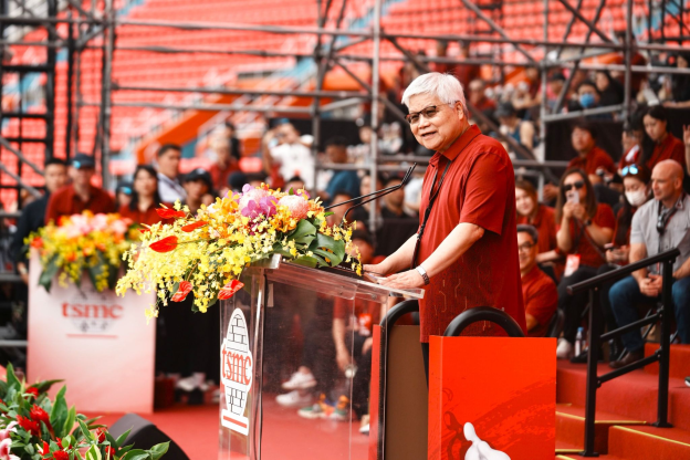
(Photo credit: TSMC)

Please note that this article cites information from WeChat account DRAMeXchange.

2024-09-03

[News] Samsung and TSMC Unlikely to Be Buyers for Intel’s Rumored Foundry Business Sale

As Intel has reportedly been working out options to navigate the company through crisis, its possible moves are said to include selling off Altera, putting a halt to its investment project in Germany, and though, less unlikely, sale of its foundry business. However, if this restructuring does happen, according to South Korean media outlets The Korea Times and The Korea Herald, Samsung and TSMC are unlikely to be buyers for Intel’s foundry operations.

A Risky Move for Samsung to Make

Intel’s thoughts on its foundry business has been casting ripples in the global semiconductor industry, as the market has been speculating who the buyers might be and whether the falling giant will take action on the potential divestiture of its foundry operations.

Nevertheless, a report by The Korea Times notes that as Intel’s foundry market share is currently small, the impact to its competitors may be minimum. Therefore, it is unlikely that this sale will immediately boost Samsung’s chip market share.

According to TrendForce’s latest analysis, top five rankings in the foundry sector remained unchanged in the second quarter, with TSMC (62.3%), Samsung (11.5%), SMIC (5.7%), UMC (5.3%), and GlobalFoundries (4.9%) stood steadfast in their positions.

Moreover, industry officials cited by the report notes that it could be a risky move for Samsung to make another large investment in Intel’s foundry. Samsung’s non-memory chip division, which encompasses foundry and large-scale system integration devices, reportedly incurred an operating loss of 300 billion won (USD 2.24 million) in the second quarter of this year, according to the report.

On the other hand, Washington’s attitude could also pose a challenge for current market players like TSMC and Samsung, the report indicates. Given that the U.S. regards semiconductor manufacturing as a matter of national security, GlobalFoundries might be the most likely buyer, as it is a U.S. company and aligns with the policy of protecting U.S. national security, according to a semiconductor industry official cited by the report.

An Emerging Foundry Opportunity for Samsung: AI Chips

A report by The Korea Herald observes that Samsung, in a way, has been facing similar difficulties with Intel, as the company finds it challenging in securing significant orders from big techs. While TSMC is known for having close ties with tech giants, Samsung, on the other hand, is seeing increased orders from startups and automotive firms.

However, a turning point may have arrived. IBM unveiled its new AI chips for servers, the IBM Telum II Processor and IBM Spyre Accelerator, at Hot Chips 2024 last week. The report notes that these upcoming chips will be manufactured by Samsung using its 5nm process technology.

The report further suggests that it would be more advantageous for Samsung to focus on identifying potential clients in the AI industry and securing their orders, rather than trying to compete with TSMC on all areas of the logic chips sector.

Read more

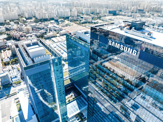
(Photo credit: Samsung)

Please note that this article cites information from The Korea Times and The Korea Herald.
2024-09-03

[News] Nanjing, China Achieved Breakthrough in Manufacturing Key SiC Chip for the First Time

As per a recent announcement by Nanjing Release, the National Third-Generation Semiconductor Technology Innovation Center (Nanjing) has successfully developed a key technology for the manufacturing of trench-type silicon carbide (SiC) MOSFET chip after four years of independent research. This breakthrough surpasses the performance limitations of planar SiC MOSFET chip, marking the first achievement of its kind in China.

SiC is one of the main representatives of wide bandgap semiconductor materials, characterized by its wide bandgap, high critical breakdown electric field, high electron saturation velocity, and high thermal conductivity. SiC MOSFET primarily comes in two structures: planar and trench, predominantly the former in current SiC MOSFET chip field.

Planar SiC MOS structure features simple process, good cell consistency, and relatively high avalanche energy. However, it faces the issue of JFET effect caused when current is confined to a narrow N-region near the P-body, which increases the on-resistance, and the large parasitic capacitance.

Trench structure refers to embedding the gate into the substrate to form a vertical channel, which allows for increased cell density, elimination of the JFET effect, optimal channel mobility, and significantly reduced on-resistance compared to planar structure. However, the trench process is more complex, with poorer cell consistency and lower avalanche energy.

“The key lies in the process,” explained Huang Runhua, Technical Director at the National Third-Generation Semiconductor Technology Innovation Center (Nanjing).

He noted that SiC is extremely hard, so converting from a planar to a trench structure means “digging a trench” in the material, which must be done with precision to avoid unevenness. During fabrication, the etching process’s precision, etching damage, and residual surface materials critically impact the development and performance of SiC devices.

To address these issues, the Innovation Center organized a core R&D team along with a full support team, and finally established a novel process flow following four years of continuous experimentation with new processes.

They overcame the challenges of precise, stable trench etching and successfully manufactured trench-type SiC MOSFET chip, improving conduction performance by about 30% compared to planar type.

The center is currently developing trench-type SiC MOSFET chip, with the goal of launching trench-type SiC power devices within a year, which are expected to be introduced to applications such as electric vehicle drivetrains, smart grids, photovoltaic energy storage.

What impact does this breakthrough have on our lives and the semiconductor industry? Huang explained, using electric vehicle as an example, that SiC power devices inherently offer power-saving advantages over silicon devices, potentially increasing lifespan by about 5%, and trench structure allows for designs with even lower resistance.

With the same conduction performance, this enables a higher-density chip layout, reducing chip usage costs.

Now, the National Third-Generation Semiconductor Technology Innovation Center (Nanjing) has already started research on SiC superjunction devices. “This structure outperforms the trench-type structure and is currently under development,” Huang Runhua revealed.

Read more

(Photo credit: DRAMeXchange)

Please note that this article cites information from WeChat account DRAMeXchange.

2024-09-03

[News] TSMC to Build Third Fab in Japan? The Timing May Be Reportedly after 2030

Taiwanese Minister of Economic Affairs J.W. Kuo, who was invited to visit Japan, attended a forum on August 30 organized by the Taiwan-Japan Research Institute and delivered a keynote speech. As reported by Kyodo News citing the interview with Kuo, he indicated that TSMC plans to build a third fab in Japan, but with a projected timeline after 2030.

However, Kuo emphasized that the final decision on whether to proceed with the expansion in Japan rests with TSMC, and he refrained from discussing specific site locations.

In addition, in response to Kuo’s comments, the Ministry of Economic Affairs clarified that any details regarding TSMC’s potential third fab should be confirmed with the foundry giant itself.

Reportedly, Kumamoto Prefecture Governor Takashi Kimura visited TSMC’s headquarters on the afternoon of August 26 and held talks with TSMC’s senior executives.

Notably, Takashi Kimura, who took office in April, stated in an report from Bloomberg on May 11th that he would spare no effort to persuade TSMC to establish a third fab in the region, believing that during the preparations for TSMC’s first fab in Kumamoto, the region already possesses better-quality road and water infrastructure and an education system that better supports international school students, which could be advantageous.

TSMC’s fabs in Kikuyo Town, Kumamoto Prefecture (Kumamoto Fab 1) is set to begin mass production in Q4 (October-December), utilizing 28/22nm and 16/12nm process technologies, with a monthly production capacity of 55,000 wafers.

The Kumamoto Fab 2 is scheduled to begin construction at the end of 2024, with the goal of starting operations by the end of 2027, focusing on 6/7nm processes. The combined monthly production capacity of TSMC’s Kumamoto fab 1 and 2 is estimated to exceed 100,000 wafers.

TSMC Chairman C.C. Wei mentioned in June that after the successful operation of the first and second fabs, TSMC would consider building a third fab if it receives the approval of the local residents.

Read more

(Photo credit: TSMC)

Please note that this article cites information from Kyodo News and Bloomberg.

  • Page 6
  • 52 page(s)
  • 259 result(s)

Get in touch with us