Popular Keywords


IC Manufacturing, Package&Test
News
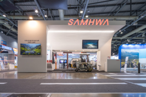
[News] Samhwa Paint Enters Semiconductor Materials with Melt Master Batch in Samsung AP Packaging
Riding the semiconductor surge, traditional industries are racing to pivot into the booming sector. South Korea’s paint giant, Samhwa Paint Industries, announced on March 6 that, in partnership with Samsung SDI, it has successfully developed high-performance MMB (Melt Master Batch), a key material...
News
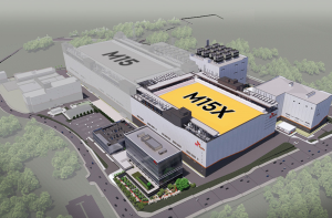
[News] Asia’s Chipmakers Reportedly Eye $136B Spend in 2026, Up 25% YoY, Spanning Foundry and Memory
Fueled by soaring demand for AI chips, memory, and logic processors, Asia’s top chipmakers are ramping up their 2026 capital spending. Nikkei and TrendForce report that leading semiconductor firms across South Korea, Taiwan, Japan, and China plan to invest over $136 billion this year, a 25% increa...
News
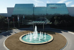
[News] Delay at Samsung’s Taylor Reportedly Slips Mass Production to 2027, Raising Concerns for Tesla
As Samsung accelerates fab approvals and equipment installations, questions are emerging about the pace of mass production at the Taylor plant. Korea JoongAng Daily reports that the start of full-scale production at Samsung’s Texas facility is now expected to slip to early 2027. If confirmed, t...
News
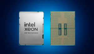
[News] Intel Unveils Xeon 6+ Clearwater Forest at MWC with 18A Chiplet Design and Foveros Direct 3D
Just weeks after unveiling Panther Lake at CES in January, Intel returned to the spotlight at MWC 2026 with the Xeon 6+ “Clearwater Forest,” showcasing the progress of 18A. According to TechPowerUp, the processor features one of Intel's most advanced chiplet designs yet: the package combines 12 ...
News
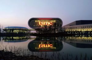
[News] TSMC’s 2025 Overseas Split: China Leads Profits, Arizona Turns Profitable, Japan Losses Widen
While NVIDIA, taking over Apple, reportedly claimed the top spot as TSMC’s largest customer, accounting for 19% of 2025 revenue, all eyes are also on the earnings performance of the company’s overseas fabs. According to Mirror Media, citing TSMC’s 2025 annual report, the Arizona plant turned p...
- Page 9
- 179 page(s)
- 892 result(s)