Popular Keywords


Semiconductors
Insights

[Insights] NVIDIA’s US$2B Marvell Deal: What’s the Strategic Significance for CPO and AI Interconnects?
NVIDIA announced on March 31, 2026 that it has entered a strategic partnership with Marvell and will invest US$2 billion, a move expected to support the development of next-generation AI and optical interconnect technologies. According to TrendForce, the collaboration goes beyond Marvell joining the...
News
[News] Samsung 2nm Yields Reportedly at ~55%, Below Mass Production Threshold; Qualcomm May Opt for TSMC
Samsung’s 2nm yield challenges are resurfacing. According to Busan Ilbo, sources indicate that Samsung Foundry’s 2nm yields remain in the mid-50% range, falling short of the roughly 60% threshold typically required for stable mass production. After backend processing, effective yields are expec...
News
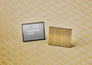
[News] Samsung Reportedly Lifts HBM4 Logic Die Prices by 40–50% Amid AI Boom; 4nm at Full Capacity
Memory is not the only segment where Samsung Electronics is pushing price increases amid surging AI demand. According to Financial News, the chip giant has reportedly raised prices for HBM4 logic dies by around 40–50% since early 2026, signaling a broader normalization of pricing across its semico...
News
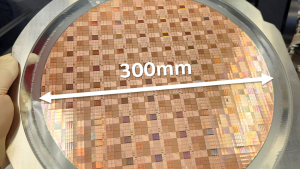
[News] Intel Launched World’s First Thinnest GaN Chiplet
On April 9, Intel Foundry Services announced a major technological breakthrough with the development of the world’s thinnest gallium nitride (GaN) chiplet. The silicon substrate has been reduced to just 19 micrometers—approx. one-fifth the diameter of a human hair. The chiplet is fabricated o...
News

[News] Apple Foldable Supply Chain Takes Shape: Samsung, Foxconn, Chinese Suppliers in Focus
With several months still to go before Apple’s fall launch event, discussions around its first foldable iPhone are already heating up rapidly. Though Nikkei notes that Apple’s first foldable iPhone has encountered technical bottlenecks during engineering testing, raising delay risks, Bloomberg r...
- Page 4
- 722 page(s)
- 3609 result(s)