Popular Keywords


Semiconductors
News
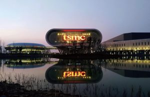
[News] TSMC 1Q Profit Seen Up ~50% to Record; Meta–Broadcom AI Chips Reportedly Target 2nm, CoWoS-L in 1H27
Ahead of its earnings call later today, TSMC is poised to capture incremental orders from the newly announced Meta Platforms–Broadcom AI chip alliance. According to Commercial Times, the partners are targeting the launch of a self-developed chip based on TSMC’s 2nm process as early as 1H27, pair...
News

[News] Intel Reportedly to Brief Staff on TeraFab Involvement in Coming Weeks, While Key Foundry Details Remain Limited
Musk’s TeraFab initiative has sparked broad industry discussion, and Intel’s decision to join the project has further intensified attention. According to CRN, Intel plans to brief employees in the coming weeks on the “scope and nature” of its involvement in the TeraFab chip manufacturing pro...
News
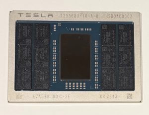
[News] Musk Confirms AI5 Tape-Out, but Wrong TSMC Tag Triggers Social Media Mix-Up
While Tesla is collaborating with Intel on its ambitious Terafab project, the company has also reached a key milestone in its next-generation AI chip program. According to Tesla CEO Elon Musk on X, the AI5 chip has officially completed tape-out. As previously reported by TechPowerUp, Tesla opts t...
News
[News] China Reportedly Sees Record 2025 Chip Tool Imports from Singapore, Malaysia; U.S. Hit Lowest Since 2017
As U.S. curbs continue to reshape supply chains, China is accelerating its push for semiconductor self-sufficiency and increasingly sourcing critical chipmaking tools from outside the U.S. According to Nikkei, imports of such equipment from Malaysia and Singapore surged in 2025, surpassing shipments...
News
[News] ASML Raises 2026 Sales Outlook to €36B–€40B on Memory, Logic Demand; South Korea Share Hits 45%
Amid an AI-driven capex upcycle among memory and logic customers, ASML has raised its 2026 revenue outlook. The Dutch chipmaking tool giant now expects sales to reach €36 billion to €40 billion (US$42–47 billion), up from its previous forecast of €34 billion to €39 billion, with a gross ma...
- Page 2
- 722 page(s)
- 3608 result(s)