Popular Keywords


Semiconductors
News
[News] ASML Raises 2026 Sales Outlook to €36B–€40B on Memory, Logic Demand; South Korea Share Hits 45%
Amid an AI-driven capex upcycle among memory and logic customers, ASML has raised its 2026 revenue outlook. The Dutch chipmaking tool giant now expects sales to reach €36 billion to €40 billion (US$42–47 billion), up from its previous forecast of €34 billion to €39 billion, with a gross ma...
Insights
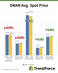
[Insights] Memory Spot Price Update: DRAM Spot Sellers Hold Firm Ahead of Mid-April Pricing, DDR4 Edges Lower 0.48%
According to TrendForce’s latest memory spot price trend report, in the DRAM segment, most spot sellers held firm on quoted prices ahead of mid-April official pricing announcements. However, weak end-demand and cautious purchasing behavior kept overall trading activity subdued. As a result, the av...
News
[News] Chinese Startup Dishan Reportedly Develops 2nm AI Chip in Prototype Verification; Foundry Access Uncertain
China may be on the verge of another advanced chip breakthrough. According to South China Morning Post, citing local outlets icrank and Shanghai Morning Post, sources say Chinese startup Dishan Technology has made progress in developing a 2nm AI chip. The company is currently in the prototype verifi...
News
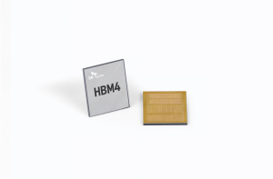
[News] HBM4 Strategies Diverge: Samsung Reportedly Chases 80% 1c DRAM Yield While SK hynix Trims Shipments by 30%
As memory giants enter the final stage of HBM4 ramp-up ahead of NVIDIA’s Rubin launch, they are taking diverging approaches. According to Chosun Biz, Samsung is pushing to lift 1c DRAM yields for HBM4 toward 80%, while ZDNet reports that SK hynix is set to cut HBM4 volumes this year by 20–30%. ...
News
[News] Korea Challenges Intel on Glass Substrate Standards as Absolics, Samsung Accelerate Commercialization
Commercialization of glass substrates is accelerating, with South Korean players and Intel increasingly competing head-on for leadership. According to Global Economic, sources indicate that Intel has laid out a glass substrate roadmap targeting 2030 to secure a technological edge, while Korean firms...
- Page 3
- 722 page(s)
- 3609 result(s)