[News] How Costly is the High-NA EUV? TSMC Reportedly Shocked, Considering Not Using the Equipment in its A16 Node
According to sources cited by a report from Economic Daily News, TSMC’s A16 advanced process node might not necessarily require ASML’s latest advanced chip manufacturing equipment, the High Numerical Aperture Extreme Ultraviolet Lithography (High-NA EUV), due to its expensive price.
Per a report from Bloomberg, during a technical symposium in Amsterdam on May 14th, TSMC’s Senior Vice President of Business Development and Co-Chief Operating Officer, Dr. Kevin Zhang, remarked that while he appreciates the capabilities of High-NA EUV, he finds its price tag to be unlikeable.
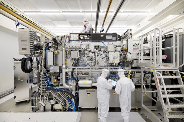
As per the same report from Bloomberg, ASML’s new machine is capable of imprinting semiconductors with lines measuring just 8 nanometers in thickness — 1.7 times smaller than the previous generation.
In terms of pricing, this EUV machine is reportedly priced at EUR 350 million (roughly USD 380 million), with a weight equivalent to two Airbus A320 passenger planes, according to Bloomberg.
Dr. Kevin Zhang stated that TSMC’s planned A16 node (scheduled for volume production slightly later in 2026) may not necessarily require the use of ASML’s High NA EUV equipment. Instead, TSMC could continue to rely on its existing, older EUV equipment. “I think at this point, our existing EUV capability should be able to support that,” he expressed.
He further mentioned that the decision to adopt the new ASML technology would depend on where it offers the most economic benefits and the technical balance they can achieve. He declined to disclose when TSMC might purchase High-NA EUV from ASML.
On the other hand, Intel has confirmed in mid-April that it has received and assembled the industry’s first High-NA EUV lithography system, which is expected to be able to print features up to 1.7x smaller than existing EUV tools. This will enable 2D feature scaling, resulting in up to 2.9x more density.
Currently, both TSMC and Samsung utilize EUV equipment for manufacturing, covering TSMC’s 7nm, 5nm, and 3nm processes and Samsung’s EUV Line (7nm, 5nm, and 4nm) located in Hwaseong, Korea, along with the 3nm GAA process.
Read more
- [News] Intel Secures First Batch of High-NA EUV Equipment from ASML, Ahead of Samsung and SK Hynix
- [News] EUV as a Strategic Asset in the Most Advanced Processes: Progress in Intel/TSMC/Samsung’s Adoptions
(Photo credit: ASML)
Please note that this article cites information from Economic Daily News and Bloomberg.


