Popular Keywords


DRAM
Insights
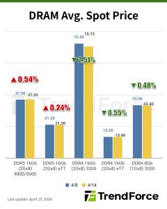
[Insights] Memory Spot Price Update: DRAM Spot Sellers Hold Firm Ahead of Mid-April Pricing, DDR4 Edges Lower 0.48%
According to TrendForce’s latest memory spot price trend report, in the DRAM segment, most spot sellers held firm on quoted prices ahead of mid-April official pricing announcements. However, weak end-demand and cautious purchasing behavior kept overall trading activity subdued. As a result, the av...
Insights
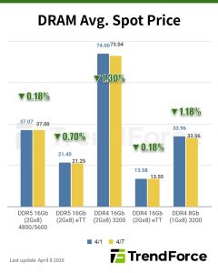
[Insights] Memory Spot Price Update: DRAM Extends Gradual Downtrend on Contained Selling Pressure; DDR4 Drops 1.18%
According to TrendForce's latest memory spot price trend report, DRAM continues to face contained selling pressure, with spot prices maintaining a gradual downward trend. In the NAND segment, most sellers are expecting further increases in 2Q26 contract prices, in an attempt to lift spot prices as w...
Insights
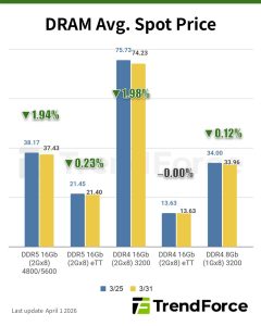
[Insights] Memory Spot Price Update: DDR3 Strength Contrasts Weak DDR4/ DDR5 Amid High Prices, Soft Demand
According to TrendForce's latest memory spot price trend report, regarding DRAM, momentum in both DDR4 and DDR5 remains weak, as end-user demand continues to struggle with elevated price levels, while 2Q26 contract pricing has yet to be formally announced. Meanwhile, in terms of NAND, module houses ...
Insights
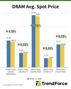
[Insights] Memory Spot Price Update: DRAM Spot Momentum Constrained as March Contracts Hold, DDR4 Weakest
According to TrendForce's latest memory spot price trend report, regarding DRAM, upward momentum in the DRAM spot market has been constrained, with the DDR4 segment being particularly weak. Meanwhile, in terms of NAND, as negotiations for contract prices of the new quarter gradually approach, the sp...
Insights
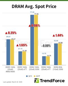
[Insights] Memory Spot Price Update: DRAM Spots Pause Amid Samsung’s March DDR4 Freeze
According to TrendForce's latest memory spot price trend report, regarding DRAM, with Samsung pausing DDR4 consumer chip price hikes in March, increases are expected to stall briefly before picking up again in 2Q26. Meanwhile, in terms of NAND, with the expectation on significant increases on contra...
- Page 1
- 46 page(s)
- 229 result(s)