Popular Keywords


ASML
News
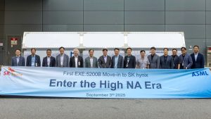
[News] ASML’s High-NA EUV for 2027-28: Which Giants Are Betting Big—Intel, Samsung, SK hynix or TSMC?
As TSMC, Intel, and Samsung kicked off 2nm mass production in late 2025, the spotlight is already shifting to their 1.4nm roadmaps and the rollout of ASML’s next-generation EUV lithography machines. According to Nikkei, citing ASML CEO Christophe Fouquet, Intel, Samsung, and SK hynix are expected ...
News
[News] ASML Posts Record €9.7B Q4 Revenue; Memory Shortage Reportedly May Boost EUV Tool Demand
ASML held its earnings call today. According to its press release, the company posted another record year in 2025, with total net sales of €32.7 billion and a gross margin of 52.8%. The fourth quarter stood out, delivering record total net sales of €9.7 billion, including revenue recognized from...
News
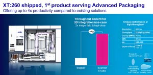
[News] Chip Tool Giants Accelerate Advanced Packaging Push, Led by ASML, Tokyo Electron, and Others
As back-end processes take on a larger role in the AI chip era, advanced packaging equipment is rising in strategic importance. According to Hankyung, leading chip equipment makers—including ASML, Applied Materials, Tokyo Electron (TEL), and Lam Research—are moving decisively into the advanced p...
News

[News] China Reportedly Builds EUV Prototype Using Older ASML Components, Eyes 2028 Chipmaking
China’s long journey toward domestic EUV lithography capability appears to be narrowing, as recent developments point to faster-than-expected progress. According to Reuters, sources say China has assembled a prototype EUV machine using components sourced from older ASML systems. As the report i...
News
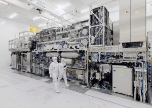
[News] Intel Completes First 2nd-Gen High-NA EUV Acceptance Testing; ASML Eyes 2027–28 Mass Production
Intel is continuing efforts to advance its foundry business and has reached another milestone with equipment supplied by Dutch lithography toolmaker ASML. According to a recent blog post from the company, Intel and ASML have completed “acceptance testing” on the first second-generation High-NA E...
- Page 3
- 22 page(s)
- 108 result(s)