Popular Keywords


ASML
News
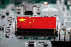
[News] Korean Expert Predicts “Chinese ASML” by 2030; Hua Hong Said to Join SMIC at 7nm
How close could China come to Western technology in AI? According to Chosun Daily, Professor Kwon Seok-joon of Sungkyunkwan University’s Department of Semiconductor Convergence Engineering said that a “Chinese ASML” could emerge within a decade. As the report notes, Kwon said China is accel...
News

[News] Meta Reportedly Eyes 20% Job Cuts, Largest Since 2023; ASML Plans 1,700 Layoffs
Major tech companies are once again preparing for layoffs. According to Reuters, sources say Meta is considering broad job cuts that could affect 20% or more of its workforce as the company seeks to offset the heavy costs of AI infrastructure investments. The report adds that no timeline has been se...
News
[News] Iran Conflict Threatens Helium for Chip: China’s Domestic Supply Push in Focus
The Iran conflict is raising concerns over the supply of key semiconductor materials. As noted by Nikkei, Middle East crisis is casting a shadow over Asia’s chip supply chain as fears grow that the de facto closure of the Strait of Hormuz could persist. Seoul is particularly concerned about helium...
News
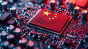
[News] “China’s ASML” by 2030? SMIC, Naura and Other Chip Leaders Call for National Effort
China has been accelerating its push for semiconductor self-reliance amid U.S. restrictions, and a new article written by the country’s leading chip executives has outlined a strategic roadmap. According to South China Morning Post, top figures in China’s semiconductor industry co-authored the p...
News
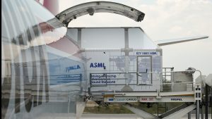
[News] ASML Reportedly Demonstrates EUV Light Source That Could Lift Chip Output 50% by 2030
ASML has unveiled a new advancement in its EUV technology that could significantly increase chip output. According to Reuters, researchers at the Dutch company have developed a way to enhance the power of EUV light source, potentially enabling up to 50% more chip production by the end of the decade....
- Page 2
- 22 page(s)
- 108 result(s)