Popular Keywords


ASE
News
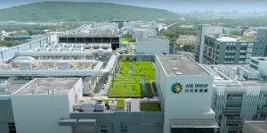
[News] ASE Reportedly to Break Ground on Six New Plants in 2026; CPO Mass Production Expected to Begin This Year
ASE Holdings, the world’s leading OSAT provider, held a groundbreaking ceremony for its new Renwu facility in Kaohsiung, presided over by CEO Tien Wu, where he also outlined the company’s expansion plans. According to TechNews, six new plants are expected to break ground worldwide this year, mar...
News
[News] Panel Maker Innolux Fab 5 Reportedly Eyed by ASE, OSAT Firms — Micron Out of Picture
AI-driven demand is fueling a new wave of capacity expansion, and the market is now suggesting that Innolux’s Nanke (Southern Taiwan Science Park) Fab 5 may be sold. According to Liberty Times, panel maker Innolux plans to sell the facility to a major semiconductor packaging and testing company, w...
News

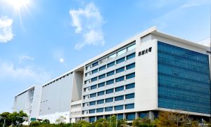
[News] ASE Buys NT$2.8B Zhunan Facility, Packaging Orders Reportedly Span NVIDIA, AMD, and More
ASE has been actively expanding on the back of AI-driven demand for advanced packaging. According to Economic Daily News, ASE has made another expansion move, with its subsidiary SPIL on the 13th spending NT$2.801 billion to acquire a plant in Zhunan, Miaoli, previously owned by United Renewable Ene...
News

[News] NVIDIA H200 Export to China Approved, Unlocking Gains for Taiwan OEMs, OSATs, and Server Suppliers
U.S. President Trump has approved the export of NVIDIA’s H200 chips to China. According to Commercial Times, industry sources say the move could accelerate inventory digestion across the AI supply chain and stimulate new orders for Taiwanese assembly and packaging providers. OEMs such as Gigabyte ...
News
[News] Chip Packaging Giant ASE Reportedly to Boost 2025 CapEx by US$1B Amid Strong AI and HPC Demand
AI is driving demand for advanced packaging, and Taiwan-based chip packaging giant ASE, which held its earnings call on the 30th, is moving quickly to ramp up operations. According to Economic Daily News, CFO Joseph Tung said the company’s 2025 capital expenditure will increase by US$1 billion to ...
- Page 1
- 9 page(s)
- 45 result(s)