Popular Keywords


ASE
News
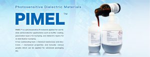
[News] Asahi Kasei Rumored to Cut PSPI Supply for Advanced Packaging, Sparks Concern for TSMC, ASE
Amid surging demand for advanced packaging, key materials are now hot commodities for tech giants. According to EE Times China and the Economic Daily News, Japan’s Asahi Kasei, a top PSPI (photosensitive polyimide) supplier to semiconductor firms like TSMC and Samsung, plans to cut PIMEL shipments...
News

[News] U.S. Whitelist Shake-up Spurs China’s Order Shift, Boosts Taiwan’s OSATs & IC Firms Like ASE
As the chip war heats up, the U.S. BIS unveiled an updated semiconductor whitelist on February 4, per its website. Commercial Times reports that the list, split into IC design (IW) and packaging & foundry (PW) categories, is likely to spark a shift in chip orders from China—a boost for Taiwan�...
News

[News] 13 Advanced Packaging Facilities to Expand Capacity Significantly by 2025
On January 16, Siliconware Precision Industries (SPIL), a subsidiary of ASE Technology Holding, officially inaugurated its new advanced packaging facility at the Tanzi Science Park. SPIL also announced that three additional advanced packaging facilities are set to expand production capacity by 2025....
News

[News] Advanced Semiconductor Packaging Technologies Emerging
The rapid development of AI, HPC, and other technologies is driving higher demands for semiconductor performance and energy efficiency. Traditional packaging technologies struggle to meet the needs of the AI era, creating an opportunity for advanced semiconductor packaging technologies to shine. ...
News

[News] Micron, UMC Reportedly Eye Stake in Taiwan’s Quasi-Government Green Power Firm
According to a report from TechNews, citing Central News Agency, Taiwan's Ministry of Economic Affairs is leading the establishment of the quasi-government-owned power company, Taiwan Intelligent Electric Power. The report notes that companies such as foundry company UMC, IC packaging and testing co...
- Page 3
- 9 page(s)
- 45 result(s)