Popular Keywords


Amkor
News
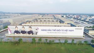
[News] Samsung Reportedly Bets on Vietnam with $4B Chip Packaging Push; Amkor Expands Presence
Semiconductor giants are accelerating global advanced packaging expansion as demand for AI chips surges, with Southeast Asia emerging as one of the most sought-after hubs. While Intel is set to bring its advanced packaging facility in Malaysia online later this year, Bloomberg reports that Samsung i...
News
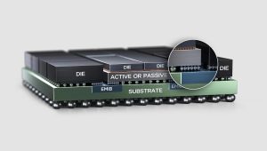
[News] Intel Reportedly Taps Amkor’s Songdo Facility for EMIB Packaging in First-Ever Outsourcing Move
Buzz is building as tech giants like Google and Meta consider Intel’s EMIB advanced packaging, and Team Blue is going full throttle. ETNews reports that Intel is understood to have established its EMIB process at Amkor's Songdo K5 facility in South Korea—its first-ever move to outsource such hig...
News

[News] Amkor Breaks Ground on USD 7 Billion Advanced Semiconductor Packaging Facility in Arizona
Chip packaging and testing giant Amkor Technology has officially broken ground on its new advanced packaging campus in Peoria, Arizona, marking a major expansion of its U.S. manufacturing footprint. Amkor initially planned to invest USD 2 billion to build a packaging and testing plant in the Fiv...
News

[News] NVIDIA Reportedly Asks Samsung, Amkor, and Foxconn to Pause H20 Production Amid China Talks
Caught between the newly lifted U.S. export restrictions and China’s pressure on domestic firms not to use the H20, NVIDIA has reportedly asked key suppliers to pause production of the China-focused AI chip, according to Reuters, citing The Information. As per the reports, the U.S. chipmaker to...
News
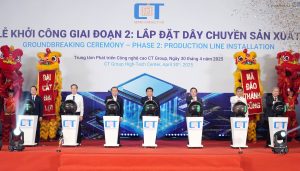
[News] Vietnam’s Semiconductor Packaging & Testing Industry Picks up Steam
Phase II of CT Semiconductor’s Packaging and Testing Plant Underway As per Vietnam’s published semiconductor development strategy, the country has set specific goals for 2030 and 2050. By 2030, Vietnam aims to establish at least 100 chip design companies, one small-scale semiconductor manufac...
- Page 1
- 7 page(s)
- 31 result(s)