Popular Keywords


SMIC
Insights
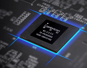
[Insights] Cambricon Remains China’s Top AI Chip Startup; Rumored 2026 Triple Output Faces SMIC Limits
Just ahead of President Trump’s approval of NVIDIA’s H200 exports to China, Bloomberg reported that rising AI chip contender Cambricon Technologies is aiming to more than triple its AI chip output in 2026 as competition with Huawei intensifies. TrendForce cautions, however, that intense compe...
News
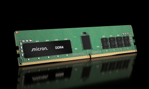
[News] Memory Crunch Ripples Across Chip Supply Chain: SMIC, NVIDIA, Device Makers Feel the Hit
As the global AI data-center race drains memory supply, major chipmakers are moving fast — and the shockwaves are spreading. Notably, Reuters reported last Friday that Samsung has quietly raised prices on select memory chips by as much as 60% from September. But the scope of this memory supercycle...
News

[News] Memory Shortage Reportedly Triggers Order Caution from Smartphone Clients, Pressuring SMIC
China's foundry giant SMIC reported robust Q3 results with profits surging 29% year-on-year, but surprised markets by revealing an unexpected ripple effect: tight memory chip supplies are making smartphone clients increasingly cautious with orders, according to chinastarmarket.cn. Notably, SMIC�...
News
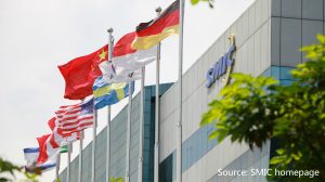
[News] SMIC Posts 29% Year-on-Year Jump in Q3 Profit, Warns of Softer Q4 Margins
Amid China’s aggressive drive for chip self-reliance, leading foundry SMIC delivered stronger-than-expected third-quarter results, The Wall Street Journal reports. The company posted net profit of $191.8 million for the period—up 29% from a year earlier and comfortably ahead of the $161.2 millio...
News
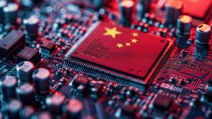
[News] SMIC Reportedly Rations Output as China Faces Widening AI Chip Crunch
Beijing’s latest push for tech self-reliance might be backfiring. After reportedly ordering all state-backed data centers to use only domestic AI chips—effectively shutting out NVIDIA—China could now be facing a deepening chip crunch. According to The Wall Street Journal, the shortage has beco...
- Page 4
- 22 page(s)
- 106 result(s)