Popular Keywords


Articles
News

[News] Samsung Reportedly in Talks for Google 2nm TPU I/O Die Order; 2028 Mass Production Eyed
Google is reportedly considering Samsung for part of its next-generation AI processor production. According to Business Korea, citing The Information, the company is discussing plans to have Samsung Foundry manufacture key components for its 10th-generation Tensor Processing Unit (TPU). Under the pr...
News

[News] Micron Taps Bechtel, Intel Ohio Fab Builder, to Speed Up New York Mega Fab Construction
Micron, which broke ground on its New York mega fab in January, has now moved to accelerate the project by naming its lead contractor. According to syracuse.com, engineering and construction giant Bechtel—also in charge of Intel’s Ohio semiconductor campus—will handle the engineering, procurem...
News

[News] From Rare Earth-Free Magnets to New Supply Chains: The Push to Break China’s Grip Accelerates
China's tighter rare earth export restrictions are accelerating efforts to reduce dependence on the country's supply chain. According to The Wall Street Journal, companies are pursuing a range of alternatives, from rare earth-free magnets and magnet-free electric motors to new magnet designs that re...
News
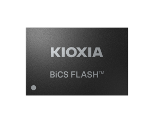
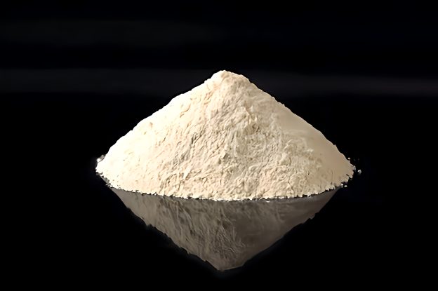
[News] The Race to 400-Layer NAND: Roadmaps and Key Technologies Driving Samsung, SK hynix, and Kioxia
As SK hynix reportedly targets mass production of 375-layer NAND by year-end, according to The Elec, the 400-layer threshold is increasingly seen as a key technical frontier in advanced NAND scaling. Against this backdrop, ET News notes that Samsung began mass producing its 286-layer NAND in Apri...
News

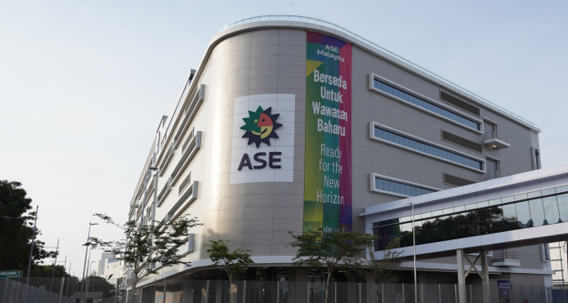
[News] ASE’s SPIL Acquires NT$2.8B Plant Amid Spillover Demand from TSMC Advanced Packaging Capacity Crunch
As AI-driven demand continues to strain advanced packaging and testing capacity, SPIL, a subsidiary of ASE, is accelerating its expansion efforts. According to Investor.com, the company has acquired Taiwan Mask Corporation's Zhunan Plant 6 for NT$2.8 billion. Because the facility is already operati...
- Page 3
- 978 page(s)
- 4890 result(s)