


[News] ASE’s SPIL Breaks Ground on Nearly TWD 100B Plant in Douliu to Boost CoWoS Capacity, Operations Set for 2028
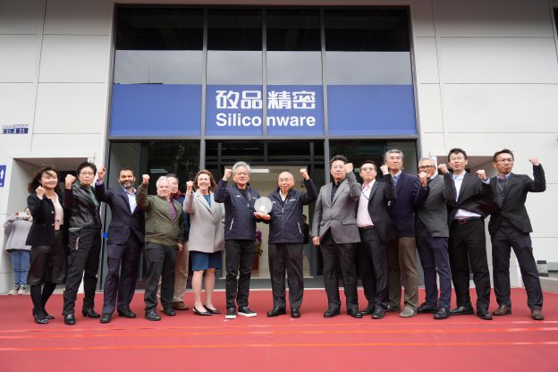
Competition in AI advanced packaging is heating up, with ASE subsidiary SPIL accelerating capacity expansion. According to Commercial Times, SPIL broke ground on August 11 on a nearly TWD 100 billion, 6-hectare plant in Douliu, Yunlin, which will introduce CoWoS advanced packaging and begin first-phase operations in 2028. The company has invested TWD 200 billion over the past two years to capture growing AI and high-performance computing (HPC) demand.
The Douliu project builds on SPIL’s broader footprint across Taiwan. Economic Daily News notes that the company began investing ahead of the AI boom by building new facilities and acquiring existing plants, with the first phase of its Huwei plant already profitable after opening last September. Vice Chairman Y.J. Chang added that SPIL still needs more land and could invest further in Yunlin if additional sites become available.
With Douliu joining Huwei as SPIL’s two major Yunlin production bases, Commercial Times notes that the company is strengthening its advanced packaging footprint alongside operations in Taichung, Changhua, Hsinchu, and Tainan.
SPIL Raises Capital for AI Packaging Push
SPIL is also raising additional capital to support its expansion. Central News Agency notes that ASE announced on behalf of SPIL that its board approved a cash capital increase to meet foreign-currency funding needs for material purchases. SPIL plans to issue 809.7 million new shares, raising TWD 16.194 billion. Industry sources cited by the report say the capital increase is primarily aimed at expanding packaging and testing capacity for AI chips.
The push comes as SPIL deepens its ties with major AI chipmakers. As Central News Agency highlights, NVIDIA CEO Jensen Huang attended the opening of SPIL’s Tanzi facility in January 2025, while institutional investors cited by the report point to the companies’ long-standing partnership in back-end packaging for HPC and AI chips.
SPIL is also working with AMD on next-generation packaging technology. In late May, AMD announced that it is collaborating with ASE, SPIL, and other industry partners to develop and validate next-generation wafer-based 2.5D bridge interconnect technology, according to Central News Agency.
TSMC CoWoS Expansion Opens More Opportunities for SPIL
Meanwhile, according to Commercial Times, TSMC Vice President of Advanced Packaging Technology and Service Jun He said TSMC’s 5.5×-reticle-size CoWoS has entered high-volume production, with yields exceeding 98% for multiple AI customer products. The company expects CoWoS to scale to 14× reticle size by 2029. As the report indicates, TSMC’s CoWoS capacity has nearly doubled annually over the past three years, and the company now operates 10 advanced packaging facilities. Institutional investors estimate that TSMC’s monthly CoWoS capacity could reach 140,000 wafers by the end of 2026 and 220,000 wafers by the end of 2027.
As CoWoS continues to scale, TSMC is also broadening its advanced packaging outsourcing. According to ETNews, sources say the company has decided to expand outsourcing of CoW (Chip-on-Wafer), a key step in CoWoS packaging for AI chips, to OSAT providers including ASE.
TSMC is continuing to invest heavily in capacity. According to Central News Agency, its board approved a US$29.4425 billion capital budget on August 11 for advanced-node, advanced packaging, and specialty process capacity, as well as fab construction and infrastructure. Of total capital expenditure, 10% to 20% will be allocated to advanced packaging, testing, mask making, and other areas.
Read more
- [News] TSMC’s 5.5-Reticle CoWoS Reportedly Tops 99% Yield; Flags Memory, ABF as AI Bottlenecks
- [News] TSMC Reportedly Expands Outsourcing of Key CoWoS Front-End Step to OSATs Amid Rising NVIDIA, ASIC Demand
(Photo credit: ASE)


