Popular Keywords
About TrendForce News
TrendForce News operates independently from our research team, curating key semiconductor and tech updates to support timely, informed decisions.
[News] TSMC Reportedly Doubles Lithography Patents From 2016 to 2023, Extending Lead Over Rivals
EUV lithography has become the cornerstone of advanced chip manufacturing, and as the foundry race intensifies at ever-smaller nodes, major players are accelerating the development of related technologies. According to Nikkei XTECH, TSMC has significantly ramped up its patent filings in semiconductor lithography technology. Between 2016 and 2023, the number of applications nearly doubled, widening the gap with Samsung and Intel. Samsung, however, has also expanded its filings since the early 2020s.
The report analyzes patent applications filed in Japan, the U.S., Europe, China, and other regions, focusing on those categorized under the IPC code “H01L21,” which covers semiconductor lithography equipment, along with patents containing the keywords “Lithography” and “EUV.”
Notably, TSMC’s patent filings under the H01L21 classification have risen sharply since the mid-2010s, outpacing other major semiconductor makers. According to the report, TSMC filed 1,548 such patents in 2023 — about 2.1 times the 723 filed in 2016.
In addition, patents including the keyword “Lithography” followed a similar trend. The report notes that TSMC filed 932 such applications in 2023, representing a 2.7-fold increase from 350 in 2016.
Beyond TSMC, the report highlights an unexpected player making strides in lithography patents — IBM. Although the American company exited semiconductor manufacturing in 2014, it has continued developing advanced process technologies, including lithography, at its Albany, New York research center. The report also notes that in the development of 2nm-generation technology, IBM has formed a partnership with Rapidus, a Tokyo-based semiconductor firm.
Samsung Ramps Up EUV Technology Development and Localization
Samsung has also been actively advancing EUV-related technologies. As noted by The Elec, the company jointly filed a patent with blank mask manufacturer S&S Tech for a pellicle frame used in EUV lithography. The patent describes a magnet-based frame assembly designed to attach pellicles to EUV photomasks.
At present, Samsung Electronics relies heavily on Japan’s Hoya Corporation for EUV blank masks but is working with S&S Tech to localize production. According to The Elec, sources indicate that Samsung aims to achieve domestic mass production of EUV blank masks by the end of this year.
Read more
- [News] Intel Rumored to Purchase more ASML High-NA EUV Equipment
- [News] Samsung Reportedly Purchasing Two ASML High-NA EUV Tools for Mass Production by 1H26
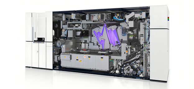
(Photo credit: ASML)
Please note that this article cites information from Nikkei XTECH and The Elec.