[News] TSMC’s 4nm Process Powers NVIDIA’s Blackwell Architecture GPU, AI Performance Surpasses Previous Generations by Multiples

Chip giant NVIDIA kicked off its annual Graphics Processing Unit (GPU) Technology Conference (GTC) today, with CEO Jensen Huang announcing the launch of the new artificial intelligence chip, Blackwell B200.
According to a report from TechNews, this new architecture, Blackwell, boasts a massive GPU volume, crafted using TSMC’s 4-nanometer (4NP) process technology, integrating two independently manufactured dies, totaling 208 billion transistors. These dies are then bound together like a zipper through the NVLink 5.0 interface.
NVIDIA utilizes a 10 TB/sec NVLink 5.0 to connect the two dies, officially termed NV-HBI interface. The NVLink 5.0 interface of the Blackwell complex provides 1.8 TB/sec bandwidth, doubling the speed of the NVLink 4.0 interface on the previous generation Hopper architecture GPU.
As per a report from Tom’s Hardware, the AI computing performance of a single B200 GPU can reach 20 petaflops, whereas the previous generation H100 offered a maximum of only 4 petaflops of AI computing performance. The B200 will also be paired with 192GB of HBM3e memory, providing up to 8 TB/s of bandwidth.
NVIDIA’s HBM supplier, South Korean chipmaker SK Hynix, also issued a press release today announcing the commencement of mass production of its high-performance DRAM new product, HBM3e, with shipments set to begin at the end of March.
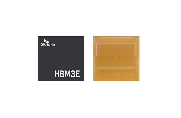
Source: SK Hynix
Recently, global tech companies have been heavily investing in AI, leading to increasing demands for AI chip performance. SK Hynix points out that HBM3e is the optimal product to meet these demands. As memory operations for AI are extremely fast, efficient heat dissipation is crucial. HBM3e incorporates the latest Advanced MR-MUF technology for heat dissipation control, resulting in a 10% improvement in cooling performance compared to the previous generation.
Per SK Hynix’s press release, Sungsoo Ryu, the head of HBM Business at SK Hynix, said that mass production of HBM3e has completed the company’s lineup of industry-leading AI memory products.
“With the success story of the HBM business and the strong partnership with customers that it has built for years, SK hynix will cement its position as the total AI memory provider,” he stated.
Read more
- [News] Foxconn Capitalizes on AI Opportunities? Reportedly Looking at Apple’s AI Server Market, B200 Also Poised to Succeed
- [News] NVIDIA and AMD Clash in AI Chip Market, as TSMC Dominates Orders with Strong Momentum in Advanced Processes
(Photo credit: NVIDIA)
Please note that this article cites information from TechNews, Tom’s Hardware and SK Hynix.


