Popular Keywords


SK Hynix
News
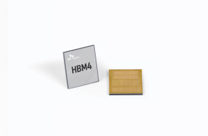
[News] HBM4 Strategies Diverge: Samsung Reportedly Chases 80% 1c DRAM Yield While SK hynix Trims Shipments by 30%
As memory giants enter the final stage of HBM4 ramp-up ahead of NVIDIA’s Rubin launch, they are taking diverging approaches. According to Chosun Biz, Samsung is pushing to lift 1c DRAM yields for HBM4 toward 80%, while ZDNet reports that SK hynix is set to cut HBM4 volumes this year by 20–30%. ...
News

[News] From Annual Deals to 3–5 Year LTAs: Samsung and SK hynix Reportedly Reset Big Tech Memory Contracts
As memory emerges as a critical bottleneck in hyperscalers’ in-house AI chip development and large-scale infrastructure buildouts, long-term supply agreements are rapidly becoming the new industry standard—on time horizons longer than previously anticipated. According to Aju News, Samsung and SK...
News

[News] Decoding Impact: Asia Chipmakers Move to Tackle Helium Strain as Intel Gains Relative Buffer
While Iran and the U.S. have agreed to a ceasefire contingent on guaranteed safe passage through the Strait of Hormuz, the helium crisis across the semiconductor supply chain shows temporary signs of easing. However, as highlighted by Forbes, Qatar’s Ras Laffan Industrial City, which supplies r...
News
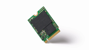
[News] SK hynix Begins Shipping Industry-First 321-Layer QLC cSSD; Supplies Dell in April
As memory giants accelerate the phase-out of legacy NAND like MLC, they are doubling down on next-generation, high-performance storage to ride the AI wave. On April 8, SK hynix announced it has begun shipping its latest cSSD, PQC21 — the first in the industry to feature 321-layer QLC NAND flash. ...
News

[News] Samsung Reportedly Solves SOCAMM2 Warpage, May Gain Edge Over Micron, SK hynix in Mass Production Timeline
Samsung has reportedly resolved a key technical challenge in its SOCAMM2 design. According to ETNews, citing sources, the company has overcome the “warpage” issue, a major hurdle ahead of mass production of its next-generation AI server memory module, SOCAMM2 (System on Chip Advanced Memory Modu...
- Page 1
- 77 page(s)
- 383 result(s)