Popular Keywords


Samsung
News

[News] Samsung Reportedly Halts Mexico Investments, Plans 30% Job Cuts Under Trump Tariff Pressure
According to a report from ijiwei, citing WAVY-TV, Samsung has decided to halt any future investments in Mexico due to uncertainties surrounding Trump's proposed tariffs, as noted by Roberto Vega Solís, president of Mexico’s Business Confederation in Tijuana. Moreover, the company has annou...
News

[News] Samsung Rumored to Mull on Scrapping 1.4nm Node to Prioritize 2nm/3nm Yield Gains
As Samsung is eager to stem losses in its foundry business, the latest market rumor indicates that the company might plan to cancel its 1.4nm node, according to Techspot and Wccftech. Citing remarks from tech tipster @Jukanlosreve, Wccftech suggests that the move could be made due to foundry stru...
News

[News] Samsung Secures Patent for Rollable Display Phone with Movable Camera
According to the Chinese media outlet IT Home, citing My Smart Price, Samsung has been granted a new patent that describes a unique display design equipped with a movable camera. The patent number is D1066344. As noted in the report, the patent showcases a rollable smartphone equipped with a sing...
News

[News] Samsung Reportedly Teams Up with Apple for Next-Gen LPW DRAM, Eyes 2028 Mass Production
As Samsung advances HBM3E validation with key clients like NVIDIA, it is also targeting the next-gen mobile DRAM market. According to The Bell, the company is developing Low Power Wide I/O (LPW) DRAM with multiple partners, including Apple, to meet the growing demand for on-device AI. The Bell in...
News

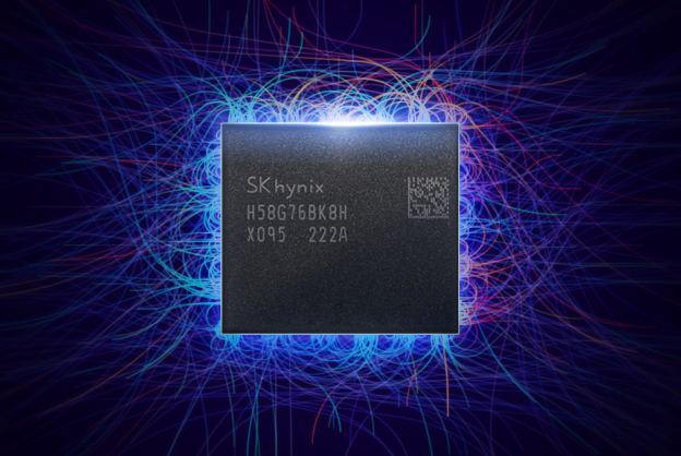
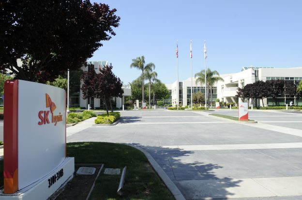
[News] Samsung & SK Hynix Post Strong 2024 Sales in China, Driven by China’s “Old-for-New” Policy
According to a report from Commercial Times, citing Yonhap News, China’s “Old-for-New” Policy, which promotes consumer trade-ins for new products, helped drive significant growth for South Korean semiconductor companies, Samsung Electronics and SK Hynix, in the Chinese market in 2024. Meanw...
- Page 47
- 146 page(s)
- 729 result(s)