ASML’s EUV (Extreme Ultraviolet Lithography) technology is widely regarded as the crown jewel of modern industry. China has attempted to break through by committing resources in a “Manhattan Project” style effort, only to find that the true barrier does not lie merely in replicating equipment, but in the global supply chain and the high volume manufacturing (HVM) data feedback loop that ASML has built over three decades. Why does China’s reverse engineering fail when faced with EUV? The answer may lie in the evolution of exposure wavelengths.
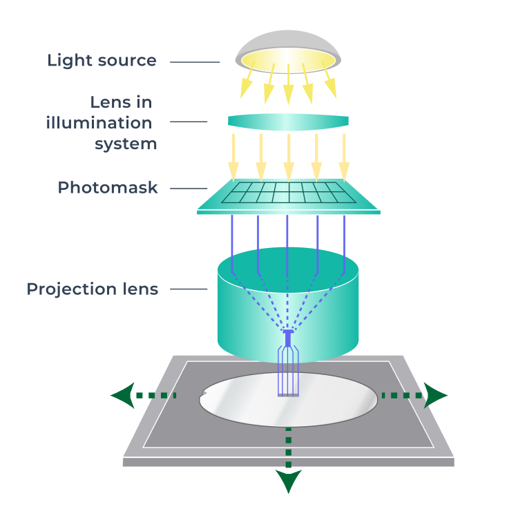
In semiconductor manufacturing, the lithography machine serves as the core equipment in the lithography process. It optically transfers pre designed circuit patterns onto the wafer surface through patterned photomasks and photoresist, and its precision and throughput directly determine a wafer fab’s yield and return on investment (ROI).
Figure 1. Principle of DUV Lithography Machine Technology
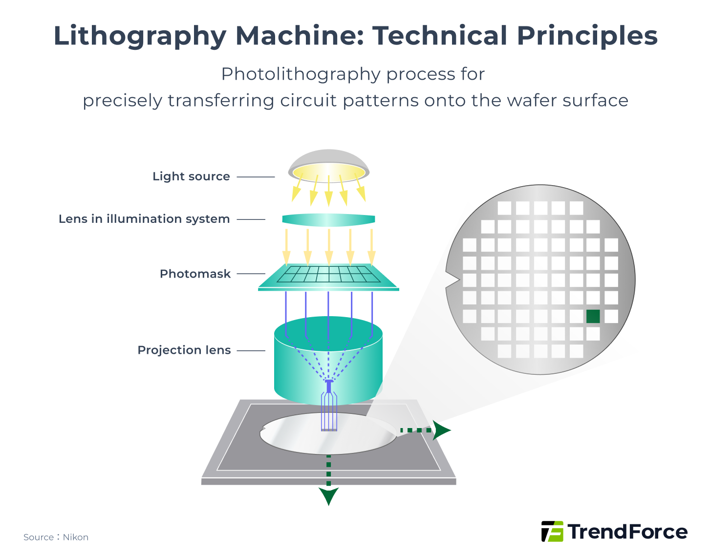
The shorter the wavelength of the light source used in lithography machines, the smaller the diffraction effect and the higher the resolution. As a result, more transistors can be packed into a given area, driving corresponding gains in chip computing performance.
Evolution of Lithography Technology: How ASML Built Its Moat
The evolution of lithography technology has essentially been a long-term race to shorten wavelengths. It progressed from early high-pressure mercury lamps (g-line, i-line) to DUV (Deep Ultraviolet Lithography), where ArF technology reduced wavelengths to 193 nm. However, a bottleneck emerged when extending the 193 nm wavelength toward the 65 nm node, and it was not until ASML and TSMC jointly developed immersion lithography machines that this barrier was overcome. This breakthrough also became the key factor that allowed ASML to widen the gap with its two other competitors, Nikon and Canon.
Immersion lithography enabled Moore’s Law to remain viable, and even today, the 7 nm node can still be developed using 193 nm immersion lithography machines. However, once process technology moves below 7 nm, the cost and yield challenges associated with DUV multiple patterning become increasingly difficult to sustain.
EUV technology has become a critical requirement for process nodes below 7 nm, and ASML has emerged as the world’s only supplier capable of EUV HVM. For this reason, the United States has actively sought to restrict access, while China has been eager to obtain EUV equipment and develop related technologies, as both sides compete for leadership in advanced semiconductor manufacturing.
Table 1. Evolution of Lithography Light Source Wavelengths and Application Nodes
| Light Source | Wavelength | Application Node | |
|---|---|---|---|
| UV | g-line | 436 nm | 250–800 nm |
| i-line | 365 nm | 250–800 nm | |
| DUV | KrF | 248 nm | 130–180 nm |
| ArF | 193 nm | 65–130 nm | |
| ArFi (Immersion) | 193 nm | 7–45 nm | |
| EUV | EUV | 13.5 nm | 3–16 nm |
Note: nm = nanometers.
(Source: TrendForce)
Figure 2. ASML EUV Lithography Technology Roadmap (1985 to Post-2030)
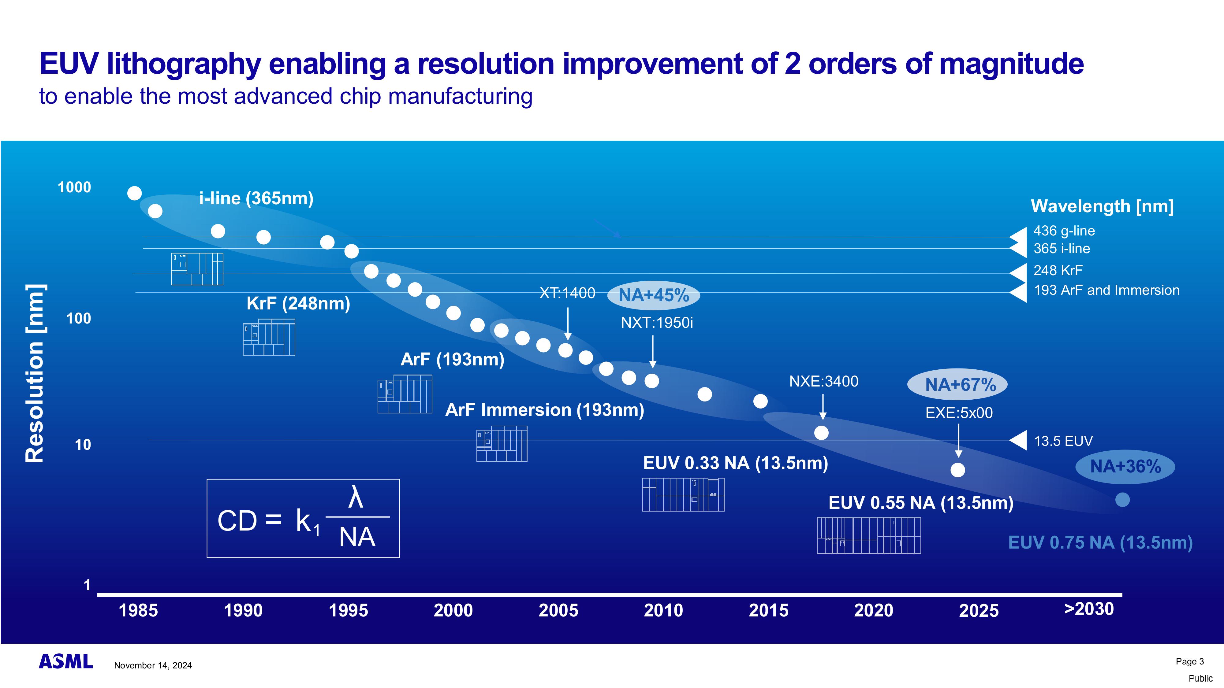
(Source: ASML’s Investor Day 2024 (Nov 14, 2024))

Breakthroughs Still Needed in Critical Equipment: China’s Alternative Paths to Advanced Chip Independence
Facing US semiconductor technology restrictions, Chinese companies are accelerating equipment self-sufficiency. Constraints on critical tools are driving a structural realignment, gradually redefining the strategic focus in response to technology controls.
In-Depth InsightsTechnical Barriers that Make EUV Difficult to Surpass
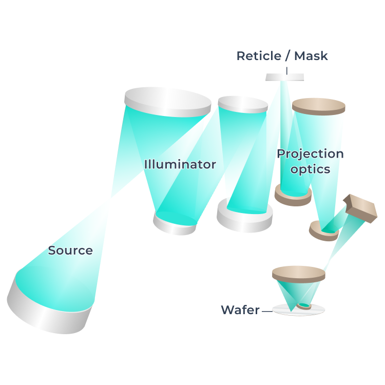
EUV uses a 13.5 nm wavelength light source, approximately 1/14 the wavelength of traditional DUV. EUV light exists only in outer space and must be artificially generated. ASML employs a Laser-Produced Plasma (LPP) method, in which a two-stage CO₂ laser hits a high-speed tin droplet, vaporizing it to generate plasma and produce the EUV light source. This process must be repeated 50,000 times per second to provide sufficient EUV exposure for wafers.
The EUV system operates in a vacuum, and light can only be guided by reflective mirrors. Therefore, the light source, mirrors, and photomasks all require redesign. This means that an EUV machine is not just a replacement of the light source, but a complete reconstruction of the optical and system engineering. EUV differs from other lithography equipment in light source, optical system, photomask, and exposure environment, each requiring around ten years of research and incremental improvements to approach HVM readiness.
Table 2. Differences Between DUV and EUV Lithography Equipment
| Comparison Item | DUV Lithography Equipment | EUV Lithography Equipment |
|---|---|---|
| Light Source | High-pressure mercury lamp → Excimer laser | Laser-excited tin plasma |
| Wavelength | 193 nm | 13.5 nm |
| Optical System | Refractive (transparent lens) | Reflective (multilayer mirror lens) |
| Exposure Environment | Normal atmosphere | Vacuum |
| Equipment Cost (USD) | $20–50M | $100–300M |
| Equipment Illustration |
|
|
(Source: TrendForce)
ASML, as the only HVM-capable EUV lithography equipment supplier, has achieved its current results through global collaboration since the 1990s. This also reflects another ASML competitive advantage—internationalized professional division of labor.
Open Innovation and Extreme Specialization Build the Lithography Technology Ecosystem
Since the mid-1990s, ASML has extensively collaborated with chip manufacturers, tool makers, and material suppliers to publish research papers. At that time, it introduced a software architecture based on Unified Modeling Language (UML), which provided a common blueprint and communication tool for internal and external scientists and engineers in a highly abstract and complex R&D environment. Leveraging internal and external R&D integration capabilities, ASML rapidly enhanced its competitive strength.
ASML’s success as the leader in EUV relies on a highly specialized division of labor, while ASML primarily focuses on R&D and final assembly. EUV lithography machines consist of over 100,000 components and weigh 180 tons, with ASML producing only about 15% of the parts. According to ASML’s official 2024 data, its global supplier network exceeds 5,150 companies, forming a large and stable supply chain. This strategy not only improves R&D efficiency but also integrates the industry’s most advanced optics, materials, and precision mechanical technologies.
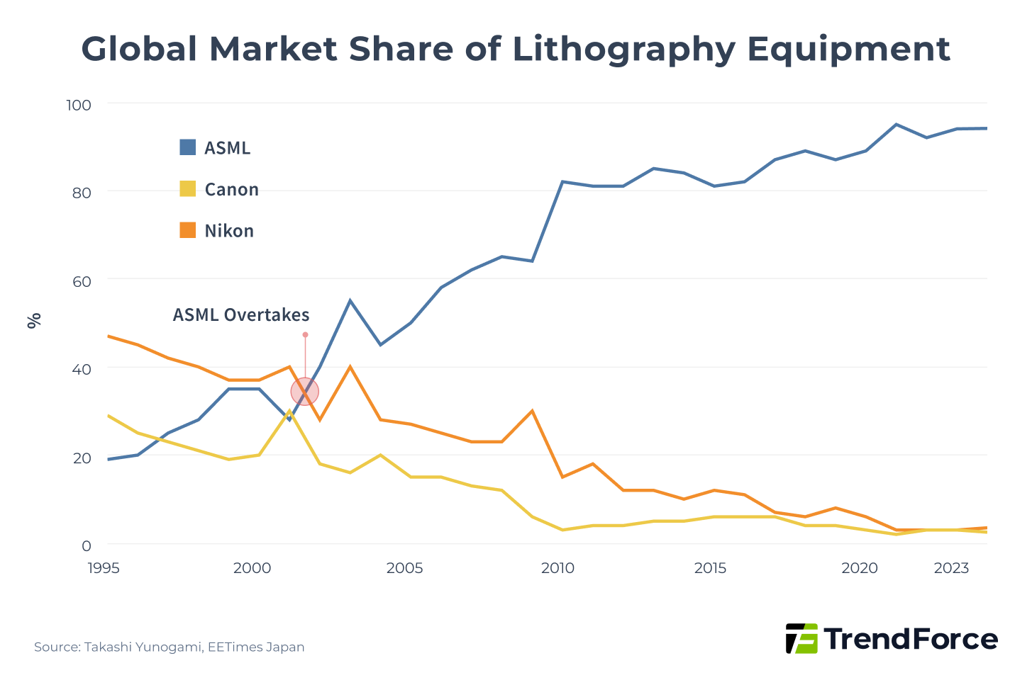
In 1998, ASML became the fastest company to transition from KrF to ArF, launching ArF lithography equipment. In 2001, it introduced the unique dual-wafer stage modular exposure system, TWINSCAN, significantly improving production efficiency and positioning accuracy. These breakthroughs enabled ASML to surpass competitors Canon and Nikon in 2002. By 2024, in the lithography equipment market, ASML held approximately 94% market share, with the remaining 6% split between Canon and Nikon, maintaining its leading position to the present day.
Figure 3. Global Lithography Equipment Market Share: ASML vs Nikon vs Canon
To ensure quality and supply stability, ASML has signed long-term cooperation agreements with key suppliers, establishing strict KPIs and quality standards, while strengthening control through technical support, training, and even acquisitions.
For example, the German optical giant Zeiss has exclusively developed the world's most precise lens modules for ASML's EUV equipment, with processing accuracy smaller than the diameter of a single silicon atom. The two companies have collaborated for over thirty years. In 2016, to deepen cooperation in EUV lithography technology, ASML acquired a 24.9% stake in Zeiss's subsidiary Carl Zeiss SMT for €1 billion in cash.
Beyond its unique and powerful system integration capabilities, ASML’s strict quality requirements and deep supplier network have established a competitive barrier that is difficult for new entrants to overcome.
Economies of Scale Driving Technological Iteration and Industry Monopoly Effects
ASML's technological evolution is not confined to its own factories but continues to iterate on production lines at major wafer fabs worldwide.
The key to the ROI of lithography equipment lies in overlay accuracy and throughput. Overlay refers to the precision with which a new layer aligns with the previous patterned layer in the lithography process. Smaller overlay errors result in higher yields, directly affecting wafer fab profitability. Throughput measures the number of exposures a machine can perform per unit time; higher throughput increases the equipment's ROI.
Most of ASML’s machines are designed for large-scale production. Each generation operates in environments where customers invest billions of dollars to process millions of production-grade wafers. This allows ASML to collect massive data on overlay precision and throughput, which is then used to improve the next-generation machines. By leveraging customer production experience to drive technological iteration, ASML benefits from an economies-of-scale learning curve that is extremely difficult for newcomers to replicate.
Additionally, the high precision required in lithography means that if all exposure steps use equipment from the same supplier, overlay errors can be maintained within optimal ranges. Mixing different brands, however, can introduce an overlay penalty due to system calibration differences, causing pattern shifts and reduced yield. For wafer fabs, such yield loss far exceeds any cost savings from procurement. Consequently, mixed equipment procurement is nearly impossible, providing ASML with a natural moat and reinforcing a winner-takes-all structure.
Precision and meticulous global professional division, strong modular development capabilities, and extensive production data experience collectively create layered barriers that form the technological wall that ASML still cannot be easily challenged.
Even if China attempts to reverse-engineer DUV machines, such efforts have ended in failure due to damage during disassembly, ultimately requiring assistance from ASML.
Industrial Automation Trends: China-US Competition in Semiconductor Industry 5.0
Amid the accelerated expansion of semiconductor manufacturing capacity, automation has emerged as a critical competitive factor. This analysis examines semiconductor production and smart manufacturing strategies in the U.S. and China, and assesses potential entry opportunities for Taiwan’s suppliers in the semiconductor automation market.
In-Depth TrendsChina’s Semiconductor Equipment Manufacturers Breaking Through Niche Markets
The semiconductor equipment market includes four segments with market sizes exceeding $10 billion, namely lithography, dry etching, visual inspection, and CVD equipment, all of which are dominated by European, American, and Japanese manufacturers.
Although China has struggled to break through in the lithography equipment market, it has gradually gained traction in the dry etching and PVD equipment segments. Led by Naura, its equipment portfolio spans etching, PVD/CVD deposition, cleaning, as well as back end testing and packaging, covering nearly all major stages of the semiconductor manufacturing process. Naura and AMEC together account for approximately 6% of the global dry etching market, while Naura’s share of the PVD equipment market reaches 12%.
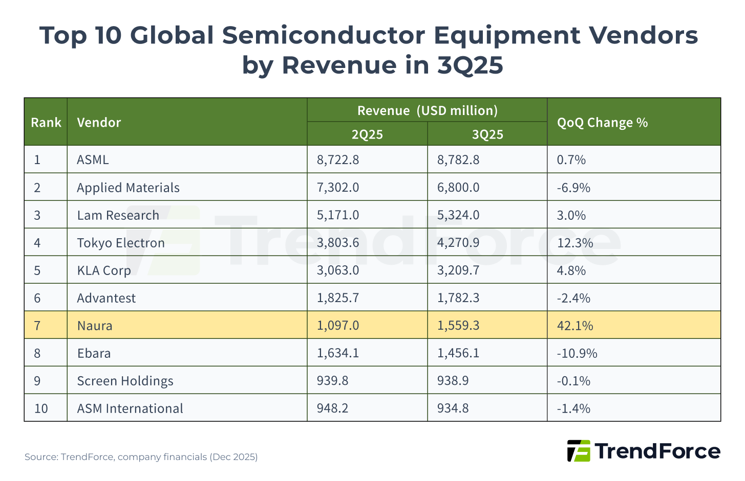
In 2023, Naura’s revenue entered the global top ten ranking for semiconductor equipment vendors. Together with AMEC and Shengmei Semiconductor, which is widely regarded as having a Chinese capital background, all three companies recorded annual revenue growth of 35% to 48% in 2024, showing notable gains in the global semiconductor equipment revenue rankings.
According to TrendForce’s latest data for Q3 2025, Naura ranks 7th globally by market share, with a quarterly growth rate of approximately 42.1%, significantly higher than other companies among the global top ten.
Figure 4. Top 10 global semiconductor equipment suppliers by revenue in 3Q25
Behind this trend is China’s massive domestic demand for semiconductor equipment. China is the world’s largest semiconductor equipment market. According to data from SEMI (Semiconductor Equipment and Materials International), semiconductor equipment investment in China reached $49.55 billion in 2024, representing a year over year increase of 35% and accounting for roughly 40% of global semiconductor equipment demand. This scale of capital investment, combined with an urgent push for self-sufficiency, has provided Chinese domestic equipment manufacturers with sufficient resources to expand and strengthen their capabilities.
Uneven Self-Sufficiency Across Equipment Segments, With Breakthroughs and Gaps
China’s semiconductor equipment industry exhibits uneven self-sufficiency rates across different subsegments, reflecting relative strength in mature process nodes and weakness in advanced process nodes. However, some segments have simultaneously made breakthrough progress in the global market.
In photoresist stripping equipment, which has the highest self-sufficiency rate among China’s domestic equipment categories, the self-sufficiency rate in the low to mid range market has reached 75% to 90%, mainly serving mature processes, power semiconductors, and advanced packaging. E-Town Semiconductor accounted for more than 30% market share in dry photoresist stripping equipment in 2023, ranking 2nd globally. However, self-sufficiency in high end photoresist stripping equipment used for 3D NAND/DRAM remains below 30%.
In cleaning and etching equipment, China’s domestic self-sufficiency rate has reached approximately 50% to 60%. AMEC’s plasma etching equipment has achieved 5 nanometer technology capability and has been adopted by leading international manufacturers, including TSMC and SK Hynix. ACM Research’s wet cleaning equipment is also qualified for use in advanced process nodes at 7 nanometers and below.
However, development in CMP, ion implantation, and lithography equipment mainly focuses on mature processes such as power semiconductors and MEMS sensors, with self-sufficiency rates ranging from approximately 10% to 25%. For advanced lithography equipment, under ASML’s monopoly, China’s domestic self-sufficiency currently approaches zero.
Figure 5. China’s Semiconductor Equipment Self-Sufficiency Rates and Leading Manufacturers
US to Cancel China Exemptions; Case Review Likely to be Approved
If the U.S. revokes technology waivers for semiconductor manufacturing in China, will China’s semiconductor supply chain be disrupted? This analysis examines the potential impacts and key areas of regulatory review.
In-Depth InsightsFrom "Single-Point Breakthrough" to "Systematic Integration"
As the United States extends export controls on advanced semiconductor equipment, China’s semiconductor equipment development strategy has undergone a fundamental shift. In addition, Chinese wafer fabs currently face hardware matching challenges in large-scale production line deployment. As previously mentioned, semiconductor manufacturing—especially lithography—requires high precision, and the adoption of equipment from different domestic suppliers increases overlay errors and yield risks. China has gradually recognized this issue.
According to TrendForce data, from January to October 2025, semiconductor manufacturers made publicly disclosed investments exceeding RMB 13 billion through private placements, capital increases, and industry funds. China has shifted from pursuing breakthrough development by individual companies to large-scale production and systematic integration.
This year, China’s semiconductor equipment leader Naura strategically invested in Xinyuan Micro, acquiring a 17.87% stake. Naura leads in etching, PVD/CVD, and cleaning equipment, while Xinyuan Micro focuses on coating, developing, and wet process equipment before and after lithography. This investment helps Naura integrate key pre- and post-lithography processes, accelerating yield improvement at Chinese wafer fabs.
China’s CMP leader Huahai Qingke formally acquired all remaining shares of Xinyu Semiconductor in April 2025. Xinyu Semiconductor provides integrated services for ion implantation equipment. Through this acquisition, Huahai Qingke moves toward equipment and service integration, covering equipment, high-precision services, and specialized consumables, seeking breakthroughs under international company monopolies.
In addition to horizontal integration, China’s equipment industry is also pursuing vertical supply chain layouts, strengthening core component manufacturing and improving domestic substitution capabilities for key components. Semiconductor material company GRINM Semiconductor acquired a 70% stake in DGT Technologies, entering the semiconductor critical materials and components sector. Equipment company JDM Jingda Machine acquired precision mold and component manufacturer Wuxi Micro Research for RMB 360 million, accelerating localization of precision components in China.
China Increases Investment in Advanced Packaging and Heterogeneous Integration
In 2025, China’s National Integrated Circuit Industry Investment Fund Phase III (referred to as Big Fund III) shifted its investment focus toward 3D packaging and heterogeneous integration.
In September, Big Fund III, through Guotou Jixin (Beijing) Equity Investment Fund, invested approximately RMB 450 million in Tuojing Jianke, a subsidiary of Piotech, Inc. focused on advanced bonding equipment. Tuojing Jianke primarily focuses on advanced bonding equipment in the 3D integration field, including hybrid bonding and fusion bonding equipment, as well as supporting measurement and inspection tools.
The performance improvement from heterogeneous integration mainly relies on advanced packaging rather than process node scaling. Industry insiders familiar with China’s semiconductor sector indicate that national strategic capital investment in 3D integration equipment is shifting toward a “More-than-Moore” technological path. This move also highlights China’s efforts to pursue breakthroughs through alternative advanced technologies beyond the traditional process miniaturization route.
China has increased investment in the semiconductor industry, with Big Fund III having a registered capital of RMB 344 billion, surpassing both Fund I (approximately RMB 130 billion) and Fund II (approximately RMB 200 billion) combined. In addition, according to market reports, parent funds in Shanghai, Beijing, Zhejiang, and Jiangsu have also launched a new round of project investments or established sub-funds. These investments cover the full semiconductor industry chain, including chip design, manufacturing, equipment, and materials.

2025 Global and China AI Data Centers: Deployment and Outlook
Rising AI compute demand is driving data centers toward GW scale. Chinese and US CSPs are diverging along global and sovereign cloud paths, with energy, grids, and policy as key constraints. This analysis highlights the latest trends in AI data center investment strategies.
In-Depth InsightsASML Hegemony and China’s Semiconductor Industry Chain Leapfrogging
ASML’s success reflects the collective achievements of the entire industry over decades in optics, materials, precision manufacturing, and global collaboration.
ASML CEO Christophe Fouquet has stated that,
China lags approximately 10 to 15 years behind in chip manufacturing, with the actual gap potentially being even larger. ASML’s leadership is not the result of a single company, but relies on an extremely complex technological ecosystem. Even if competitors can replicate the appearance of lithography machines, they cannot acquire Zeiss’s high-precision lenses, Cymer’s laser sources, TSMC’s testing platforms, or the years of accumulated precision operation data.
The most fundamental challenge faced by China’s semiconductor equipment manufacturers is the HVM learning cycle that cannot be easily overcome with money or reverse engineering. However, according to SEMI, the global semiconductor equipment market is expected to reach $127.5 billion in 2025, with China remaining the largest driver of global equipment growth.
China’s strategy is shifting. Observing the investment direction of the 2025 semiconductor fund, China has moved from previous years of blindly investing large sums and building industrial parks toward a more pragmatic, purpose-driven strategic investment. Through horizontal and vertical integration, it aims for coordinated operation and systematic optimization of the entire industry chain, establishing a more complete ecosystem.
At the same time, China is attempting to leapfrog traditional process scaling by entering areas such as 3D ICs and heterogeneous integration. The country seeks breakthroughs through alternative innovative technologies, hoping to establish its own advantages in the next round of the chip competition.