Popular Keywords


Qualcomm
News

[News] MediaTek, Qualcomm Reportedly Cut 4nm Wafer Starts, Down ~15% YoY Amid Rising Memory Costs
Surging memory prices are weighing on end demand, with smartphone demand showing signs of cooling. According to Commercial Times, the market outlook remains weak, prompting SoC vendors to scale back wafer starts, with sources saying MediaTek has begun reducing its 4nm wafer starts at foundries. Medi...
News
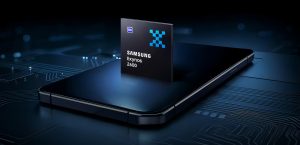
[News] Samsung Exynos 2600 Reportedly Trails Snapdragon by Up to 28% in Battery Life; 2nm Efficiency Faces Doubts
Samsung’s Exynos 2600 is reportedly facing challenges in power efficiency. According to Chosun Biz, tests conducted under identical conditions comparing the chip with Qualcomm’s Snapdragon 8 Elite Gen 5 revealed a battery life gap of up to 28%. While overall performance between the two is consid...
News

[News] Chip Giants Tighten Taiwan Links as Intel CEO Tan Headlines COMPUTEX, Qualcomm Elevates Taiwan
Please note that this article cites information from Commercial Times, Knews, Liberty Times and Diamond Rapids on X. With COMPUTEX 2026 set for early June, visits by top chip executives are taking center stage. Intel CEO Lip-Bu Tan and Qualcomm CEO Cristiano Amon are slated to deliver keynotes, wi...
News

[News] India’s Chip Ambitions Grow: Qualcomm Completes 2nm Tape-Out, MediaTek Reportedly Mulls Entry
As India ramps up its semiconductor push, smartphone chip giant Qualcomm has completed the tape-out of a 2nm chip design in the country, marking a major milestone, according to local media Business Standard. The report, citing Qualcomm, notes that the work was carried out across the company’s e...
News

[News] NVIDIA Reportedly Plans No New Gaming GPU in 2026 Amid Memory Tightness, First Time in 30 Years
NVIDIA may delay the launch of its next gaming GPU as memory supplies remain tight. According to The Information, sources say the company does not plan to release a new graphics chip for gaming this year, as a deepening global memory shortage is pushing NVIDIA to prioritize its limited memory capaci...
- Page 1
- 25 page(s)
- 125 result(s)