Popular Keywords


PSMC
News
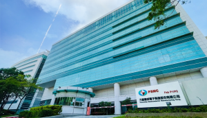
[News] PSMC Core Business Reportedly Swings to Profit in Q1; Micron Deal Adds Strategic Upside
Following Micron’s completion of its acquisition of Powerchip Semiconductor Manufacturing Corp’s Tongluo P5 fab in March, the Taiwanese chipmaker provided further operational updates. According to Central News Agency, PSMC said at its annual general meeting on April 10 that first-quarter operati...
News
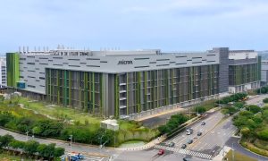
[News] Micron Reportedly Schedules March 26 Tool Move-In at PSMC Tongluo Fab, Signaling Next Deal Phase
After formally signing an exclusive letter of intent to acquire Powerchip Semiconductor Manufacturing Corp. (PSMC)’s P5 fab in Tongluo for US$1.8 billion, Micron has begun moving the deal forward. According to TechNews, the memory giant recently sent out a confidential invitation announcing a tool...
News
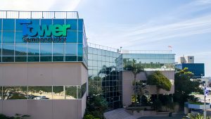
[News] Israel Unrest Disrupts Tower; Orders Reportedly Shift to Vanguard, PSMC, Lifting Mature-Node Pricing
As Israel enters a state of emergency, shipments from Israel-based foundries have reportedly been disrupted, prompting global companies to shift orders. According to Economic Daily News, Israel’s largest foundry and a top-ten global player, Tower Semiconductor, has faced shipment constraints, lead...
News

[News] PSMC Joins Intel, SoftBank’s ZAM Initiative to Manufacture AI Memory, Eyeing an Alternative to HBM
The AI boom is triggering an explosive surge in memory chip demand, putting Taiwan's PSMC in the spotlight. According to Economic Daily News, PSMC has teamed up with Intel and Japan's SoftBank Group in an AI memory collaboration, taking on a key role in pilot production and manufacturing. The cross-...
News
[News] AI Demand Blunts Foundry Seasonality: TSMC Sees 4% 1Q Growth; VIS, PSMC Raise Prices
AI demand powers foundries through the slow season. According to Central News Agency, the first quarter is traditionally a slow season for foundries, but this year is benefiting from strong AI demand alongside a recovery in panel driver IC orders. As a result, foundries including TSMC are expected t...
- Page 1
- 12 page(s)
- 58 result(s)