Popular Keywords


HBM4
News
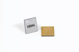
[News] HBM4 Strategies Diverge: Samsung Reportedly Chases 80% 1c DRAM Yield While SK hynix Trims Shipments by 30%
As memory giants enter the final stage of HBM4 ramp-up ahead of NVIDIA’s Rubin launch, they are taking diverging approaches. According to Chosun Biz, Samsung is pushing to lift 1c DRAM yields for HBM4 toward 80%, while ZDNet reports that SK hynix is set to cut HBM4 volumes this year by 20–30%. ...
News
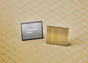
[News] Samsung Reportedly Lifts HBM4 Logic Die Prices by 40–50% Amid AI Boom; 4nm at Full Capacity
Memory is not the only segment where Samsung Electronics is pushing price increases amid surging AI demand. According to Financial News, the chip giant has reportedly raised prices for HBM4 logic dies by around 40–50% since early 2026, signaling a broader normalization of pricing across its semico...
News
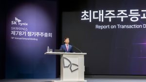
[News] SK hynix Aims to Secure ₩100T+ in Net Cash to Support Long-Term Investment; ADR Eyed for 2H26
Please note that this article cites information from SK hynix, ZDNet, Yonhap News, Chosun Ilbo, and Reuters. SK hynix held its 78th annual general shareholders’ meeting at its headquarters in Icheon on the 25th, bringing its investment strategy into focus. According to ZDNet, President Kwak No...
News

[News] Samsung Reportedly Allocates 50%+ of Pyeongtaek Foundry Capacity to HBM4 Base Die; Said to Win OpenAI Deal
Please note that this article cites information from Hankyung. Samsung is reportedly ramping HBM4 base die production at its foundry. According to Hankyung, sources say the company will allocate over half of its Pyeongtaek foundry capacity to in-house HBM4 base dies, rather than external clients. ...
News
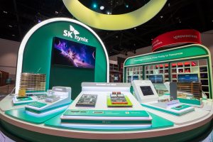
[News] SK hynix Showcases AI Memory at GTC; Chairman Warns Wafer Shortage May Last Until 2030
SK hynix is set to showcase its latest AI memory technologies at GTC 2026. In a press release, the company said it will present solutions designed to reduce data bottlenecks and boost performance for both AI training and inference within NVIDIA’s AI infrastructure. The exhibit will feature memory ...
- Page 1
- 24 page(s)
- 118 result(s)