Popular Keywords


IC Manufacturing, Package&Test
News
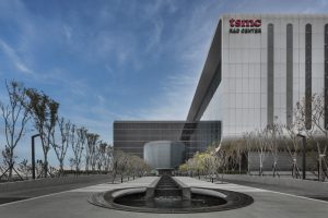
[News] TSMC Reportedly to Break Ground 1.4nm Taichung Fab on Nov. 5; Mass Production Slated in 2H28
Fresh off celebrating the first NVIDIA Blackwell wafer produced in Arizona, TSMC is ramping up its 1.4nm expansion in Taiwan. According to Economic Daily News, the company filed construction plans with the Central Taiwan Science Park Administration on October 17 and plans to break ground on November...
News
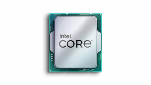
[News] Intel Reportedly Raises Prices Up to 20% for Intel 7-Based Raptor Lake, Alder Lake; Asia Market Hit Hard
While Intel has just unveiled Panther Lake, its first major product built on the 18A process, the company is reportedly raising prices for Alder Lake and Raptor Lake processors, which are manufactured on Intel 7, ijiwei reports. Earlier rumors suggested price adjustments of up to 10% for 13th-gen...
News
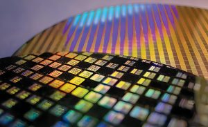
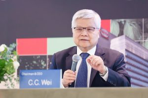
[News] TSMC Confirms N2P for 2H26, Joins A16 to Cement 2nm-Class as Major, Long-Lived Node
As TSMC races toward 2nm mass production by year-end, the foundry is rolling out fresh updates on its N2 and A16 nodes. Chairman C.C. Wei, cited by TechNews, said that while N2 remains on track, TSMC is also preparing N2P — an upgraded extension of the N2 family that promises higher performance an...
News
[News] TSMC Projects Q4 Sales Down 1% QoQ, Up 22% YoY with 60% Margin, Holds $40-42B 2025 Capex
After posting new high net profit in the third quarter, TSMC expects Q4 revenue to range between US$32.2 billion and US$33.4 billion, based on its current business outlook. Assuming an exchange rate of NT$30.6 to the U.S. dollar, management forecasts a gross profit margin of 59% to 61% and an operat...
News
[News] TSMC Posts Record Q3 Profit, EPS NT$17.44 Amid AI Surge, Tariff Concerns
TSMC today announced consolidated revenue of NT$989.92 billion, net income of NT$452.30 billion, and diluted earnings per share of NT$17.44 (US$2.92 per ADR unit) for the third quarter ended September 30, 2025. As Reuters reported, TSMC’s Q3 profit hit a record high on soaring demand for AI inf...
- Page 17
- 161 page(s)
- 805 result(s)