


[News] SK hynix, SanDisk Debut HBF Standard to Challenge AI Memory Bottlenecks with Google, Tenstorrent Support
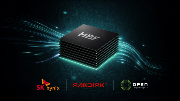
Six months after SK hynix partnered with SanDisk to drive High Bandwidth Flash (HBF) standardization, the consortium has reached a key milestone by unveiling the first HBF standard specifications. According to SK hynix, the inaugural specification supports capacities of up to 512GB using 8-high and 16-high NAND stack configurations, with three bandwidth tiers (Grade 1–3) delivering roughly 0.4TB/s to 3.0TB/s.
The announcement came at the opening of Future of Memory and Storage (FMS) 2026, held at the Santa Clara Convention Center in California from Aug. 4–6. Notably, SK hynix also aims to accelerate adoption of an open HBF ecosystem by rallying major backers including Google DeepMind, and Tenstorrent, according to SEN TV.
The specification, disclosed through the Open Compute Project (OCP), adopts the industry-standard UCIe interconnect, enabling HBF to integrate with a broad range of processors, including GPUs and CPUs. It further defines interface and electrical characteristics, HBF die-stacking reliability and packaging guidelines, as well as software I/O requirements, SK hynix said.
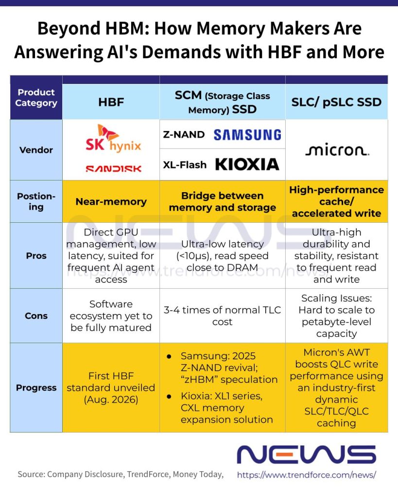
As noted by Financial News, unlike HBM, which stacks DRAM dies to maximize bandwidth, HBF stacks NAND flash to deliver a new memory tier between HBM and SSDs.
According to TrendForce, HBF is emerging as a complementary technology to HBM rather than a competing one, with the potential to address HBM’s high cost and limited capacity. Although NVIDIA has yet to announce any plans to adopt the technology, industry sentiment remains broadly positive. The interest shown by industry leaders such as Google and Tenstorrent have shown a willingness to consider adopting HBF, though specific use cases have not yet been determined.
Thus, TrendForce believes the long-term architecture will likely combine HBM for ultra-high-speed computation with HBF for high-density data storage, creating a hybrid memory hierarchy that could become a key enabler of large-scale AI commercialization.
HBF Roadmap Toward Commercialization
According to SK hynix, HBF technology is expected to reduce the total cost of ownership (TCO) while increasing the scalability of AI systems. The industry forecasts that the demand of complex memory solutions, including HBF, will pick up around 2030.
Notably, SanDisk aims to introduce HBF prototypes in the second half of this year, with Japan emerging as a leading candidate for the production site, according to an April ETNews report. A pilot production line is expected to be completed in the second half and begin operation around year-end, with commercialization targeted for 2027, the report added.
World’s First 375-Layer V10 4D NAND Slated for Early 2027
Another key highlight was SK hynix’s unveiling of the world’s first 375-layer, 10th-generation (V10) 4D NAND, with mass production scheduled for early 2027, according to the company. The memory giant said the chip delivers a 2.5x improvement in performance per watt, targeting one of data centers’ biggest challenges: power consumption.
With 375-layer NAND-based enterprise SSDs set to enter production early next year, SK hynix said it expects to complete what it describes as the industry’s only full-stack AI memory portfolio spanning DRAM (HBM), the intermediate HBF tier, and storage (eSSD).
Another highlight of the announcement would be SK hynix’s showcase of the world’s first 375-layer, 10th-generation (V10) 4D NAND, which the company plans to begin mass production in early 2027, according to its press release.
As noted by SK hynix, the product is expected to deliver a 2.5x improvement in performance per watt to directly address one of data centers’ biggest challenges, power consumption. As its 375-layer NAND-based enterprise SSDs are scheduled to enter production early next year, SK hynix is expected to complete what it says will be the industry’s only full-stack AI memory portfolio spanning DRAM (HBM), the intermediate HBF tier, and storage (eSSD).
Read more
- [News] SanDisk Goes Beyond HBF: Patent Bonds Processor onto NAND Tile, with HBM Stacks on Shared Interposer
- [News] HBF Spurs Equipment Race; Hanmi Semiconductor Eyes First TC Bonder Deliveries in 2H26
(Photo credit: SK hynix)


