[News] SanDisk Goes Beyond HBF: Patent Bonds Processor onto NAND Tile, with HBM Stacks on Shared Interposer
While SanDisk is speeding up the development of High Bandwidth Flash (HBF), a next-generation architecture that vertically stacks NAND, the company is also advancing additional memory concepts aimed at addressing structural capacity constraints.
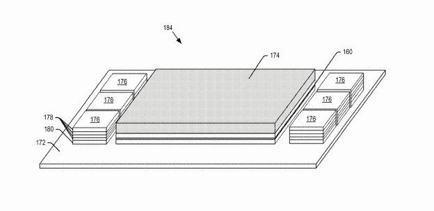
According to a U.S. patent (US 12,430,274 B2) filed and published by SanDisk earlier, the proposed design integrates a multi-core processor directly onto a CBA (CMOS Bonded to Array) memory tile — which itself combines a large NAND flash array with a CMOS logic layer.
The integrated stack is then mounted on an interposer, with stacks of HBM semiconductor dies affixed around one or more sides of the combined stack, SanDisk notes.
Rationale Behind the Design
The design rationale behind SanDisk’s approach, as noted by Wccftech, is partly driven by the inherent limitations of HBM, particularly its relatively constrained capacity, as well as the challenges that HBF has yet to fully address, including latency, power efficiency, and system-level integration complexity.
To overcome HBM’s capacity ceiling, SanDisk previously introduced its HBF architecture, which adopts a similar concept to HBM by vertically stacking multiple layers of NAND flash and connecting them via through-silicon vias (TSVs) to form a unified memory stack, according to Wccftech.
While current HBM solutions typically offer 32–64GB per stack, HBF is designed to scale significantly higher, with reported capacity reaching up to 4TB. According to SanDisk, HBF is capable of closely matching HBM’s bandwidth while delivering 8-16x the capacity of HBM at a similar cost.
However, despite NAND offering higher capacity at a lower cost, Wccftech also points out that it is positioned further from the compute die, resulting in slower data access compared to DRAM-based architectures. In response, SanDisk’s latest patent, as highlighted by the report, proposes a 3D stacking design in which a NAND flash tile, built using a CBA structure, is positioned beneath a compute tile such as an AI accelerator or GPU.
Under this configuration, HBM DRAM would still be integrated on the same interposer, but would serve a distinct role within the overall memory-compute hierarchy, according to Wccftech. As highlighted by the report, this architecture allows HBM to handle immediate, high-speed memory operations, while the NAND flash layer within the memory tile is used for read/write-intensive workloads and large-scale data storage.
Read more
- [News] HBF Spurs Equipment Race; Hanmi Semiconductor Eyes First TC Bonder Deliveries in 2H26
- [News] SanDisk Reportedly Eyes 2H26 HBF Pilot Line; May Advance Previously Announced Timeline by Half a Year
(Photo credit: SanDisk, U.S. Patent and Trademark Office)