[News] Glass Substrates Eye 2027 Launch, Scale Toward 2030 as CoWoS Costs Rise and Hyperscaler Demand Grows
As AI chips continue to scale in size and complexity, demand is rising for next-generation packaging and substrate solutions, with glass substrates emerging as a focal point. According to Sisa Journal, the technology is expected to begin early commercialization in 2027, move through a ramp-up phase by 2029, and enter full-scale mass production from 2030 onward.
Notably, the report points to NVIDIA and Google—two of the most influential players in the AI accelerator market—as the most likely end customers to drive adoption of glass substrates.
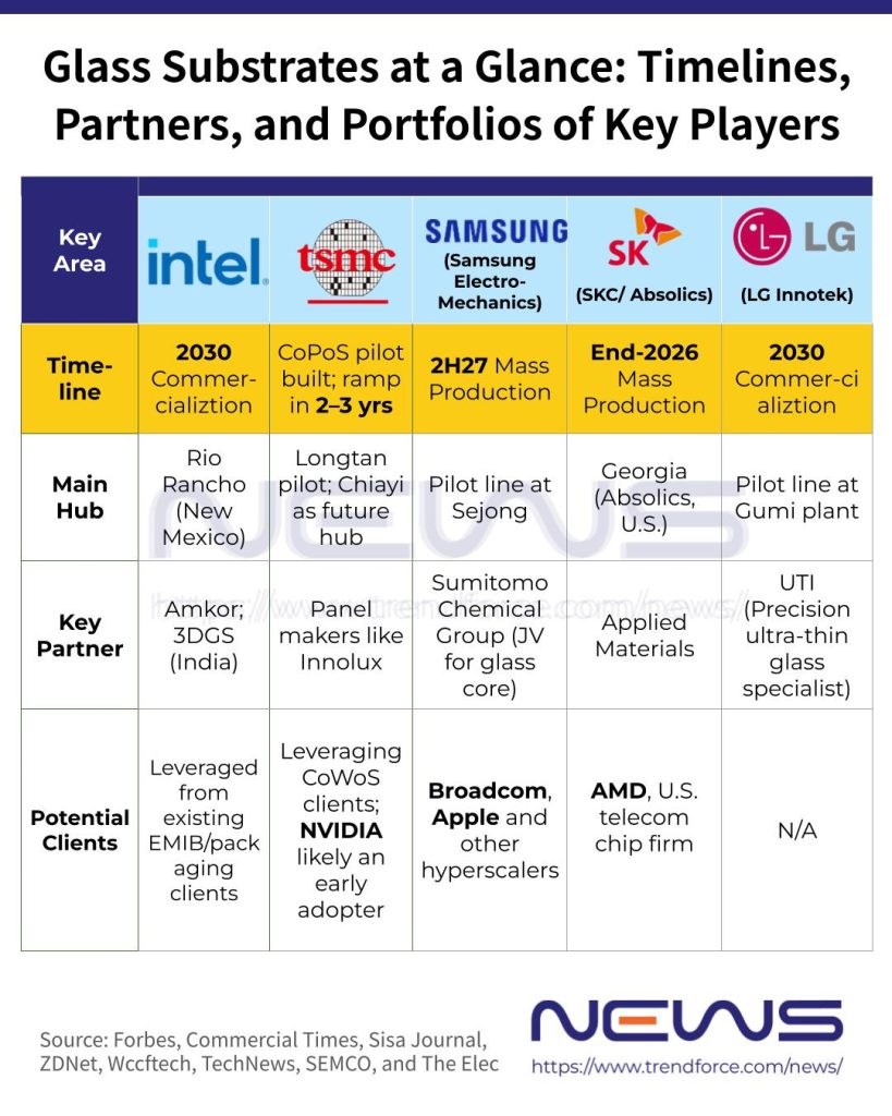
The timeline broadly aligns with remarks from TSMC Chairman C.C. Wei at the company’s June 4 shareholder meeting. Economic Daily News, citing Wei, reports that TSMC has already built a CoPoS pilot production line, with meaningful ramp-up expected in about two to three years. Separately, TrendForce’s substack highlights that TSMC introduced its 310×310 mm CoPoS (Chip-on-Panel-on-Substrate) platform in 2025, where glass is used as the interposer.
CoWoS Cost Surge Reportedly Becomes Key Catalyst
Sisa Journal highlights that strong investment from hyperscalers in next-generation infrastructure and packaging remains a key driver. As explained by the report, glass substrates are gaining traction due to better heat and warpage resistance, while the increasing need to connect GPUs and HBM at higher density over larger scales is positioning them as a scalable option.
Notably, rising costs of TSMC’s silicon-based CoWoS are seen as an additional catalyst, the report adds. An April Commercial Times report suggested that that the average selling price (ASP) of a CoWoS wafer is around $10,000, comparable to 7nm-class advanced process nodes, underscoring how advanced packaging has evolved into a high-value competitive segment.
Key Timeline and Players’ Moves
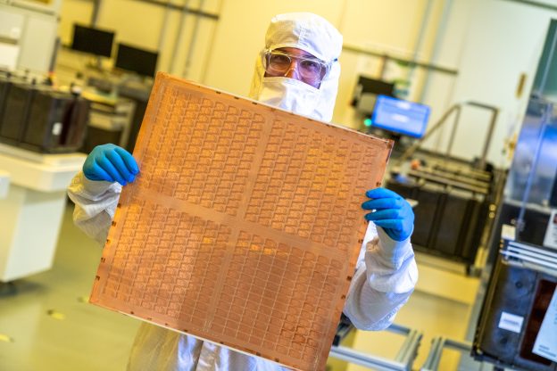
With TSMC outlining its glass substrate roadmap, Forbes reports that Intel’s Rio Rancho fab in New Mexico is producing silicon photonics for external customers. Its first glass substrate prototypes integrated with co-packaged optics (CPO) have also been showcased, with commercialization targeted around 2030, as highlighted by the report.
Meanwhile, Korean players are also making moves. Sisa Journal reports that SKC, Samsung Electro-Mechanics, and LG Innotek are accelerating commercialization efforts by conducting production qualification tests with end customers, with SKC viewed as the most aggressive investor.
As reported by The Elec, SKC completed a KRW 1.2 trillion rights offering and plans to inject an additional KRW 589.6 billion into its glass substrate subsidiary, Absolics. According to the report, Absolics has recently launched a new project, supplying prototype “non-embedding” glass substrates to a U.S. telecommunications chip company.
Absolics’ glass substrates, targeted at high-performance servers and AI accelerators, are said to reduce thickness by 25% and improve power efficiency by more than 30% compared with conventional organic interposers, according to Sisa Journal.
On the other hand, Sisa Journal notes that Samsung Electro-Mechanics is running a glass substrate pilot line at its Sejong plant in Chungnam. The company is targeting mass production in the second half of 2027 and is currently conducting quality evaluations with potential customers, including Broadcom and other major hyperscalers, the report adds.
LG Innotek is also seen as another emerging player for glass substrates. According to Sisa Journal, the company has set up a pilot line at its Gumi plant and earlier this year partnered with UTI on R&D to improve the mechanical strength of glass substrates. UTI, known for its ultra-thin glass (UTG) used in foldable smartphones such as those from Samsung Electronics, is also extending its glass processing expertise into the substrate segment, the report notes.
Read more
- [News] Intel Reportedly Eyes World’s First Glass Substrate Output at Rio Rancho; Offers Silicon Photonics to Customers
- [News] SKC Said to Speed Glass Substrate Mass Production by Year-End; Advances New Non-Embedding Tech for U.S. Client
(Photo credit: Intel)


