[News] Samsung, SK hynix Plan New Heat Dissipation Technologies Starting HBM5: Three Memory Makers’ Approaches in Focus

While Samsung Electronics and SK hynix showcase HBM5 and HBM4E respectively at COMPUTEX Taipei, competition among memory giants is increasingly centering on thermal management. As reported by The Asia Business Daily, Samsung, SK hynix, and Micron are placing greater emphasis on cooling and power-efficiency technologies, as AI chip leaders NVIDIA and AMD push HBM suppliers to enhance thermal control and low-power design capabilities.
Building on this trend, the report further highlights that power consumption of next-generation AI server GPUs from NVIDIA and other vendors is trending toward 1,000W per chip, significantly raising system-wide thermal demands.
Meanwhile, beyond overall AI chip architecture trends, the challenge is expected to intensify further as HBM stacking advances. As the industry moves beyond HBM3E toward HBM4E and HBM5, with layer counts potentially reaching around 20, thermal management is becoming an increasingly critical constraint for both performance and scalability.
Against this backdrop, The Korea Times reports that beginning with HBM5, Samsung Electronics and SK hynix are set to roll out new chip-level heat dissipation technologies aimed at curbing thermal buildup.
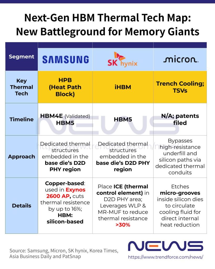
Samsung’s Approach: HPB (Heat Path Block)
Notably, Samsung showcased its HPB (Heat Path Block) technology alongside its HBM5 mock-up at COMPUTEX. According to Yonhap News, the design enhances heat dissipation by creating additional thermal pathways within the HBM structure to better manage internally generated heat. Samsung DS CTO Song Jae-hyuk noted that HPB has already been implemented in HBM4E, with reliability and stability fully validated.
The D2D PHY (die-to-die physical layer), which enables ultra-high-speed data transfer between HBM and external GPUs, is identified as a major heat source in the base die. Samsung’s HPB is reported to introduce an independent thermal path within the D2D PHY region, improving heat conduction and dissipation, lowering thermal resistance, and strengthening overall system stability.
As highlighted by The Korea Times, HPB has already been applied in application processors such as Samsung’s Exynos 2600, where a copper-based structure is placed above the AP die to create a more efficient heat-dissipation path. The approach reportedly cuts thermal resistance by up to 16%.
For HBM, however, the report—citing Song—notes that Samsung is exploring a silicon-based HPB architecture. Song emphasized that the key lies in optimizing the placement of the base die and core dies, suggesting that HPB is being integrated into the full memory-stack design rather than simply added as an upper-layer thermal solution, the report adds.
SK hynix’s Approach: iHBM with Cooling Elements
In terms of SK hynix, the company unveiled its iHBM solution, which integrates cooling elements (ICEs) directly into the HBM package. According to a late-May press release, the company plans to adopt this architecture in next-generation products, including HBM5.
Similar to Samsung’s approach, SK hynix is also addressing thermal challenges at the D2D PHY interface. Unlike conventional HBM designs that rely on heat dissipation through the core die, iHBM integrates ICEs—silicon-based materials that are thermally conductive yet electrically insulating—directly into the D2D PHY between the HBM stack and GPUs, SK hynix explains. The company claims this design reduces thermal resistance by 30% while significantly improving operational stability.
As highlighted by SK hynix, the iHBM solution adopts a structural approach to thermal management by creating an additional heat dissipation path within the package. It also leverages the company’s wafer-level packaging (WLP) process and proven MR-MUF technology to enable stable high-volume manufacturing.
Micron Takes a Different Path
On the other hand, The Asia Business Daily notes that Micron is taking a different approach from its South Korean peers in addressing thermal challenges, as the company is focusing on low-power HBM designs, primarily enabled through its through-silicon via (TSV) trench cooling technology, the report adds.
Trench cooling, as per the report, involves etching microscopic grooves into the silicon die inside AI accelerator chips and circulating cooling fluid through these channels to reduce internal heat buildup, thereby improving thermal management performance.
Beyond this specific approach, intellectual property and technology analytics platform PatSnap notes that the industry is also moving toward dedicated thermal conduits that bypass high-resistance underfill and silicon-die heat paths in 3D architectures. Multiple players — including Micron, Huawei, and major Chinese memory manufacturers — are reportedly pursuing similar design directions.
Separately, PatSnap highlights Micron’s 2025 U.S. patent on stacked memory thermal dissipation, which describes a vertical heat-management structure based on electrically passive cooling TSVs. In this design, a thermally conductive layer is embedded in the base interface die, from which TSVs extend through the full memory stack toward a heat-removal layer at the top.
These TSVs function solely as heat-conducting channels and are aligned within the same footprint as signal TSVs to avoid additional die-area penalties. Together, they form a low-resistance vertical thermal path operating in parallel with the electrical TSV network, according to PatSnap.
Read more
- [News] Samsung Unveils HBM5 Model for the First Time at Computex, Production Reportedly Seen Around 2028
- [News] SK hynix Introduces iHBM Solution, Targets HBM5 Adoption with 30% Thermal Resistance Reduction
(Photo credit: TrendForce)


